BORA SOM/BORA Evaluation Kit/pdf
Getting started[edit | edit source]
Kit Identification Codes[edit | edit source]
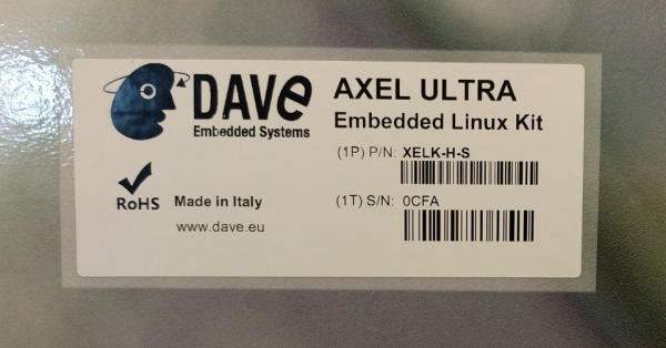
The development kits (DESK, XELK, XUELK, BELK, etc.) are identified by a couple of codes:
- P/N Part Number identification code
- S/N Serial Number identification code
These codes are printed on a label sticked to the box containing the kit.
For example, the following picture shows such a label of an Axel Ultra XELK (XELK-H-S) with Serial Number 0CFA
These codes are required to complete the registration process of the kit.
Unboxing[edit | edit source]
Once you've received the kit, please open the box and check the kit contents with the packing list included in the box, using the table on this chapter as a reference.
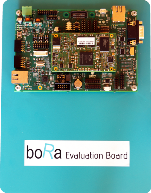
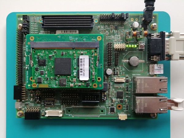
The hardware components (SOM, carrier boards and display) are pre-assembled, as shown in the picture below:
Video[edit | edit source]
Kit contents[edit | edit source]
| Component | Description | Notes |
|---|---|---|
| Bora SOM
Default option is DBRF4110S2R (see Order codes for more options)
|
| |

|
BORA Carrier board | Se also the BoraEVB page |
| AC/DC Single Output Wall Mount adapter Output: +12V – 2.0 A |
Please refer to Belk Quick Start Guide | |
| FTDI USB/RS232 cable adapter |
FTDI code: CHIPI-X10 | |
| D9 Female to D9 Female null modem cable | ||
| MicroSDHC card |
Order codes[edit | edit source]
| Order code | Description |
|---|---|
| BELK-L-S-S | This code refers to the default configuration detailed above |
microSD Layout[edit | edit source]
The microSD provided with the kit is used to store:
- a bootable partition (mmcblk0p1, vfat) containing:
- binary images (u-boot and kernel images)
- root file system partition (mmcblk0p2, ext4)
Target setup and first boot[edit | edit source]
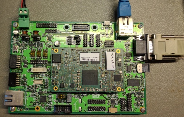
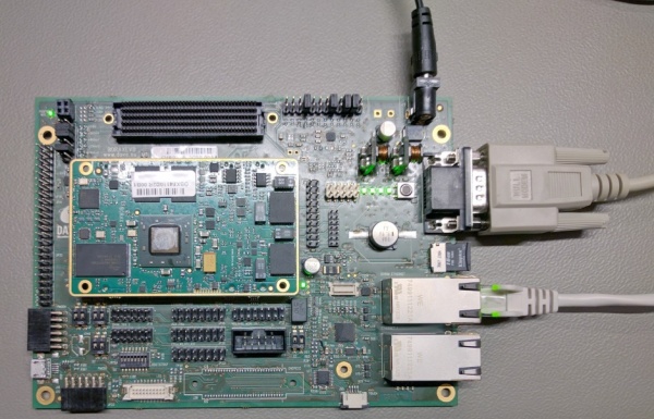
This section describes how to quickly start Bora/BoraEVB and BoraX/BoraXEVB systems included in the BELK/BXELK:
- on target side, connect a null-modem cable on J17 DB9 connector, denoted also as UART1
- on host side, connect the other end of the null-modem cable to a COM port and start your favorite terminal software that will be used to interact with the target's serial console; communication parameters are 115200-8-N-1
- optionally connect the BoraEVB/BoraXEVB board to an Ethernet LAN by plugging cable into connector J8, also denoted as ETH0 on BoraEVB and BORAX ETHERNET on BoraXEVB
- connect 12V power supply to JP2 or J7 connector, also denoted as PSU 12V
- insert the microSD card in the slot J21, also denoted as MICROSD.
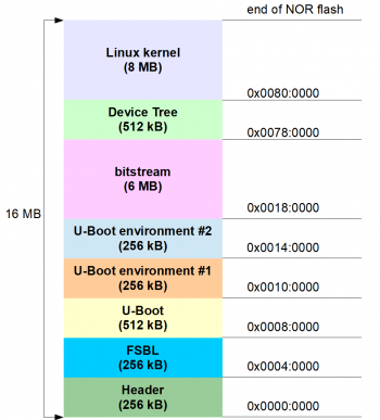
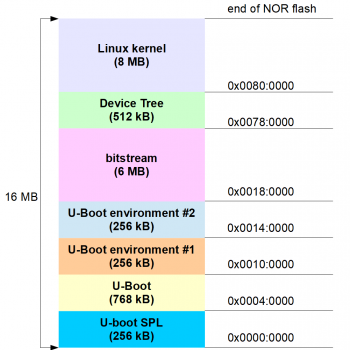
Once power has been applied to the target, FSBL or U-boot SPL and U-Boot bootloaders will be fetched from the SPI NOR flash that equips Bora/BoraX/BORA Lite SOM and executed. Boot messages will be printed out to the serial console. Redundant U-Boot environment is stored in the NOR flash as well, as depicted in the following image.
By default, U-Boot is configured to retrieve Linux kernel image stored in the microSD card [1]. In turn, Linux kernel shall mount root file system from the mmcblk0p2 partition of the microSD card itself [2], [3]. At the end of boot process, Linux shell shall be available on the serial console. Default boot process does not download any bitstream to the Programmable Logic.
The following dump shows the typical messages printed out to the console during bootstrap process. This log refers to Belk-4.0.0 running on BORA SOM. For BORAX SOM similar messages are printed out to the console.
U-Boot SPL 2017.01-belk-4.0.0 (Jul 11 2017 - 15:58:04)
qspi boot
Trying to boot from SPI


U-Boot 2017.01-belk-4.0.0 (Jul 11 2017 - 15:58:04 +0200), Build: jenkins-BELK_u-boot-10

Model: Bora
Board: Xilinx Zynq
I2C:   ready
DRAM:  ECC disabled 1 GiB
Relocating to 3ff2e000, new gd at 3eaedee8, sp at 3eaedec0
NAND:  1024 MiB
MMC:   sdhci@e0100000: 0 (SD)
SF: Detected s25fl256s_64k with page size 256 Bytes, erase size 64 KiB, total 64 MiB
*** Warning - bad CRC, using default environment

In:    serial@e0001000
Out:   serial@e0001000
Err:   serial@e0001000
Model: Bora
Board: Xilinx Zynq
SF: Detected s25fl256s_64k with page size 256 Bytes, erase size 64 KiB, total 64 MiB
SF: Detected s25fl256s_64k with page size 256 Bytes, erase size 64 KiB, total 64 MiB
SOM ConfigID#: 00000001
SOM UniqueID#: 01234567:89abcdef
ds2431_readmem(): error in chip reset
ds2431_readmem(): error in reading buffer
ds2431_readmem(): error in chip reset
ds2431_readmem(): error in reading buffer
CB ConfigID CRC mismatch for 0x00000000 (was 0x00000000, expected 0x2144df1c) at block 3 (offset 96): using default
CB ConfigID#: ffffffff
CB UniqueID#: 00000000:00000000
Net:   ZYNQ GEM: e000b000, phyaddr 7, interface rgmii-id
eth0: ethernet@e000b000
Hit ENTER within 3 seconds to stop autoboot
starting USB...
USB0:   USB EHCI 1.00
scanning bus 0 for devices... 1 USB Device(s) found
       scanning usb for storage devices... 0 Storage Device(s) found

USB device 0: unknown device
** Bad device usb 0 **
switch to partitions #0, OK
mmc0 is current device
reading boot.scr
472 bytes read in 12 ms (38.1 KiB/s)
Running bootscript from mmc ...
## Executing script at 02080000
bootscript generated with command "mkimage -A ARM -T script -C none -n BELK -d bootscript.txt boot.scr"
reading uImage
3770880 bytes read in 642 ms (5.6 MiB/s)
reading bora.dtb
10647 bytes read in 19 ms (546.9 KiB/s)
Booting Bora/BoraX via mmc
## Error: "configid_fixup" not defined
## Booting kernel from Legacy Image at 02080000 ...
   Image Name:   Linux-4.9.0-belk-4.0.0-xilinx
   Image Type:   ARM Linux Kernel Image (uncompressed)
   Data Size:    3770816 Bytes = 3.6 MiB
   Load Address: 00008000
   Entry Point:  00008000
   Verifying Checksum ... OK
## Flattened Device Tree blob at 02000000
   Booting using the fdt blob at 0x2000000
   Loading Kernel Image ... OK
   Loading Device Tree to 1effa000, end 1efff996 ... OK
Switching to NAND storage before starting Linux

Starting kernel ...

Uncompressing Linux... done, booting the kernel.
[    0.000000] Booting Linux on physical CPU 0x0
[    0.000000] Linux version 4.9.0-belk-4.0.0-xilinx (jenkins@linuxserver2) (gcc version 6.2.1 20161016 (Linaro GCC 6.2-2016.11) ) #1 SMP PREEMPT Sun Jul 9 23:10:22 CEST 2017
[    0.000000] CPU: ARMv7 Processor [413fc090] revision 0 (ARMv7), cr=18c5387d
[    0.000000] CPU: PIPT / VIPT nonaliasing data cache, VIPT aliasing instruction cache
[    0.000000] OF: fdt:Machine model: Bora
[    0.000000] bootconsole [earlycon0] enabled
[    0.000000] cma: Reserved 16 MiB at 0x3f000000
[    0.000000] Memory policy: Data cache writealloc
[    0.000000] On node 0 totalpages: 262144
[    0.000000] free_area_init_node: node 0, pgdat c0a2d840, node_mem_map ef7f7000
[    0.000000]   Normal zone: 1536 pages used for memmap
[    0.000000]   Normal zone: 0 pages reserved
[    0.000000]   Normal zone: 196608 pages, LIFO batch:31
[    0.000000]   HighMem zone: 65536 pages, LIFO batch:15
[    0.000000] percpu: Embedded 14 pages/cpu @ef7d1000 s26124 r8192 d23028 u57344
[    0.000000] pcpu-alloc: s26124 r8192 d23028 u57344 alloc=14*4096
[    0.000000] pcpu-alloc: [0] 0 [0] 1
[    0.000000] Built 1 zonelists in Zone order, mobility grouping on.  Total pages: 260608
[    0.000000] Kernel command line: root=/dev/mmcblk0p2 rootwait rw console=ttyPS0,115200n8 debug earlyprintk
[    0.000000] PID hash table entries: 4096 (order: 2, 16384 bytes)
[    0.000000] Dentry cache hash table entries: 131072 (order: 7, 524288 bytes)
[    0.000000] Inode-cache hash table entries: 65536 (order: 6, 262144 bytes)
[    0.000000] Memory: 1013220K/1048576K available (6144K kernel code, 232K rwdata, 1512K rodata, 1024K init, 323K bss, 18972K reserved, 16384K cma-reserved, 245760K highmem)
[    0.000000] Virtual kernel memory layout:
[    0.000000]     vector  : 0xffff0000 - 0xffff1000   (   4 kB)
[    0.000000]     fixmap  : 0xffc00000 - 0xfff00000   (3072 kB)
[    0.000000]     vmalloc : 0xf0800000 - 0xff800000   ( 240 MB)
[    0.000000]     lowmem  : 0xc0000000 - 0xf0000000   ( 768 MB)
[    0.000000]     pkmap   : 0xbfe00000 - 0xc0000000   (   2 MB)
[    0.000000]     modules : 0xbf000000 - 0xbfe00000   (  14 MB)
[    0.000000]       .text : 0xc0008000 - 0xc0700000   (7136 kB)
[    0.000000]       .init : 0xc0900000 - 0xc0a00000   (1024 kB)
[    0.000000]       .data : 0xc0a00000 - 0xc0a3a1a0   ( 233 kB)
[    0.000000]        .bss : 0xc0a3a1a0 - 0xc0a8afb4   ( 324 kB)
[    0.000000] Preemptible hierarchical RCU implementation.
[    0.000000]  Build-time adjustment of leaf fanout to 32.
[    0.000000]  RCU restricting CPUs from NR_CPUS=4 to nr_cpu_ids=2.
[    0.000000] RCU: Adjusting geometry for rcu_fanout_leaf=32, nr_cpu_ids=2
[    0.000000] NR_IRQS:16 nr_irqs:16 16
[    0.000000] efuse mapped to f0802000
[    0.000000] slcr mapped to f0804000
[    0.000000] L2C: platform modifies aux control register: 0x02060000 -> 0x02460000
[    0.000000] L2C: DT/platform modifies aux control register: 0x02060000 -> 0x02460000
[    0.000000] L2C-310 erratum 769419 enabled
[    0.000000] L2C-310 enabling early BRESP for Cortex-A9
[    0.000000] L2C-310 full line of zeros enabled for Cortex-A9
[    0.000000] L2C-310 dynamic clock gating enabled, standby mode enabled
[    0.000000] L2C-310 cache controller enabled, 8 ways, 512 kB
[    0.000000] L2C-310: CACHE_ID 0x410000c8, AUX_CTRL 0x46460001
[    0.000000] zynq_clock_init: clkc starts at f0804100
[    0.000000] Zynq clock init
[    0.000000] ps_clk frequency not specified, using 33 MHz.
[    0.000012] sched_clock: 64 bits at 333MHz, resolution 3ns, wraps every 4398046511103ns
[    0.007870] clocksource: arm_global_timer: mask: 0xffffffffffffffff max_cycles: 0x4ce07af025, max_idle_ns: 440795209040 ns
[    0.018886] Switching to timer-based delay loop, resolution 3ns
[    0.024887] clocksource: ttc_clocksource: mask: 0xffff max_cycles: 0xffff, max_idle_ns: 537538477 ns
[    0.033937] timer #0 at f080c000, irq=17
[    0.038252] Console: colour dummy device 80x30
[    0.042581] Calibrating delay loop (skipped), value calculated using timer frequency.. 666.66 BogoMIPS (lpj=3333333)
[    0.053061] pid_max: default: 32768 minimum: 301
[    0.057843] Mount-cache hash table entries: 2048 (order: 1, 8192 bytes)
[    0.064345] Mountpoint-cache hash table entries: 2048 (order: 1, 8192 bytes)
[    0.071973] CPU: Testing write buffer coherency: ok
[    0.076890] CPU0: thread -1, cpu 0, socket 0, mpidr 80000000
[    0.082484] Setting up static identity map for 0x100000 - 0x100058
[    0.258340] CPU1: thread -1, cpu 1, socket 0, mpidr 80000001
[    0.258442] Brought up 2 CPUs
[    0.266979] SMP: Total of 2 processors activated (1333.33 BogoMIPS).
[    0.273360] CPU: All CPU(s) started in SVC mode.
[    0.278941] devtmpfs: initialized
[    0.285288] VFP support v0.3: implementor 41 architecture 3 part 30 variant 9 rev 4
[    0.293052] clocksource: jiffies: mask: 0xffffffff max_cycles: 0xffffffff, max_idle_ns: 19112604462750000 ns
[    0.303669] pinctrl core: initialized pinctrl subsystem
[    0.310015] NET: Registered protocol family 16
[    0.316110] DMA: preallocated 256 KiB pool for atomic coherent allocations
[    0.358364] cpuidle: using governor ladder
[    0.398352] cpuidle: using governor menu
[    0.414905] hw-breakpoint: found 5 (+1 reserved) breakpoint and 1 watchpoint registers.
[    0.422775] hw-breakpoint: maximum watchpoint size is 4 bytes.
[    0.428739] zynq-ocm f800c000.ocmc: ZYNQ OCM pool: 256 KiB @ 0xf0880000
[    0.435584] zynq-pinctrl 700.pinctrl: zynq pinctrl initialized
[    0.455610] vgaarb: loaded
[    0.458851] SCSI subsystem initialized
[    0.462817] usbcore: registered new interface driver usbfs
[    0.468276] usbcore: registered new interface driver hub
[    0.473587] usbcore: registered new device driver usb
[    0.479680] pps_core: LinuxPPS API ver. 1 registered
[    0.484514] pps_core: Software ver. 5.3.6 - Copyright 2005-2007 Rodolfo Giometti <giometti@linux.it>
[    0.493700] PTP clock support registered
[    0.499357] clocksource: Switched to clocksource arm_global_timer
[    0.520290] NET: Registered protocol family 2
[    0.525350] TCP established hash table entries: 8192 (order: 3, 32768 bytes)
[    0.532409] TCP bind hash table entries: 8192 (order: 4, 65536 bytes)
[    0.538840] TCP: Hash tables configured (established 8192 bind 8192)
[    0.545202] UDP hash table entries: 512 (order: 2, 16384 bytes)
[    0.551082] UDP-Lite hash table entries: 512 (order: 2, 16384 bytes)
[    0.557542] NET: Registered protocol family 1
[    0.562207] RPC: Registered named UNIX socket transport module.
[    0.567985] RPC: Registered udp transport module.
[    0.572752] RPC: Registered tcp transport module.
[    0.577445] RPC: Registered tcp NFSv4.1 backchannel transport module.
[    0.583922] PCI: CLS 0 bytes, default 64
[    0.588414] hw perfevents: enabled with armv7_cortex_a9 PMU driver, 7 counters available
[    0.598056] futex hash table entries: 512 (order: 3, 32768 bytes)
[    0.604966] workingset: timestamp_bits=30 max_order=18 bucket_order=0
[    0.612013] jffs2: version 2.2. (NAND) (SUMMARY)  © 2001-2006 Red Hat, Inc.
[    0.619910] bounce: pool size: 64 pages
[    0.623630] io scheduler noop registered
[    0.627583] io scheduler deadline registered
[    0.631928] io scheduler cfq registered (default)
[    0.639167] dma-pl330 f8003000.dmac: Loaded driver for PL330 DMAC-241330
[    0.645763] dma-pl330 f8003000.dmac:         DBUFF-128x8bytes Num_Chans-8 Num_Peri-4 Num_Events-16
[    0.654861] e0000000.serial: ttyPS1 at MMIO 0xe0000000 (irq = 145, base_baud = 3125000) is a xuartps
[    0.664307] e0001000.serial: ttyPS0 at MMIO 0xe0001000 (irq = 146, base_baud = 3125000) is a xuartps
à[    0.673432] console [ttyPS0] enabled
[    0.673432] console [ttyPS0] enabled
[    0.680527] bootconsole [earlycon0] disabled
[    0.680527] bootconsole [earlycon0] disabled
[    0.689751] xdevcfg f8007000.devcfg: ioremap 0xf8007000 to f086f000
[    0.696648] [drm] Initialized
[    0.712609] brd: module loaded
[    0.723100] loop: module loaded
[    0.728406] libphy: Fixed MDIO Bus: probed
[    0.735460] CAN device driver interface
[    0.741807] libphy: MACB_mii_bus: probed
[    0.840108] macb e000b000.ethernet eth0: Cadence GEM rev 0x00020118 at 0xe000b000 irq 148 (00:50:c2:1e:af:e0)
[    0.849977] Micrel KSZ9031 Gigabit PHY e000b000.etherne:07: attached PHY driver [Micrel KSZ9031 Gigabit PHY] (mii_bus:phy_addr=e000b000.etherne:07, irq=-1)
[    0.864140] e1000e: Intel(R) PRO/1000 Network Driver - 3.2.6-k
[    0.869913] e1000e: Copyright(c) 1999 - 2015 Intel Corporation.
[    0.876782] ehci_hcd: USB 2.0 'Enhanced' Host Controller (EHCI) Driver
[    0.883279] ehci-pci: EHCI PCI platform driver
[    0.887820] usbcore: registered new interface driver usb-storage
[    0.894012] e0002000.usb supply vbus not found, using dummy regulator
[    0.900703] ULPI transceiver vendor/product ID 0x0424/0x0006
[    0.906275] Found SMSC USB331x ULPI transceiver.
[    0.910910] ULPI integrity check: passed.
[    0.916630] mousedev: PS/2 mouse device common for all mice
[    0.922521] i2c /dev entries driver
[    0.926190] cdns-i2c e0004000.i2c: 100 kHz mmio e0004000 irq 142
[    0.933517] rtc-ds3232 0-0068: oscillator discontinuity flagged, time unreliable
[    0.943182] rtc-ds3232 0-0068: rtc core: registered ds3232 as rtc0
[    0.950800] ina2xx 0-0041: power monitor ina226 (Rshunt = 10000 uOhm)
[    0.959126] Xilinx Zynq CpuIdle Driver started
[    0.964011] sdhci: Secure Digital Host Controller Interface driver
[    0.970180] sdhci: Copyright(c) Pierre Ossman
[    0.974447] sdhci-pltfm: SDHCI platform and OF driver helper
[    1.039420] mmc0: SDHCI controller on e0100000.sdhci [e0100000.sdhci] using DMA
[    1.047063] usbcore: registered new interface driver usbhid
[    1.053610] usbhid: USB HID core driver
[    1.060557] nand: device found, Manufacturer ID: 0x01, Chip ID: 0xd3
[    1.066828] nand: AMD/Spansion S34ML08G1
[    1.070797] nand: 1024 MiB, SLC, erase size: 128 KiB, page size: 2048, OOB size: 64
[    1.079104] Bad block table found at page 524224, version 0x01
[    1.086183] Bad block table found at page 524160, version 0x01
[    1.092800] 8 ofpart partitions found on MTD device pl35x-nand
[    1.098568] Creating 8 MTD partitions on "pl35x-nand":
[    1.103708] 0x000000000000-0x000000040000 : "nand-SPL"
[    1.120695] 0x000000040000-0x000000100000 : "nand-uboot"
[    1.137009] 0x000000100000-0x000000140000 : "nand-uboot-env1"
[    1.153846] 0x000000140000-0x000000180000 : "nand-uboot-env2"
[    1.160646] mmc0: new SDHC card at address 0001
[    1.165619] mmcblk0: mmc0:0001 SD16G 14.6 GiB
[    1.170685] 0x000000180000-0x000000780000 : "nand-bitstream"
[    1.177693] 0x000000780000-0x000000800000 : "nand-device-tree"
[    1.183599]  mmcblk0: p1 p2
[    1.194709] 0x000000800000-0x000001000000 : "nand-linux"
[    1.211164] 0x000001000000-0x000020000000 : "nand-rootfs"
[    1.232466] NET: Registered protocol family 17
[    1.236842] can: controller area network core (rev 20120528 abi 9)
[    1.243084] NET: Registered protocol family 29
[    1.247450] can: raw protocol (rev 20120528)
[    1.251720] can: broadcast manager protocol (rev 20161123 t)
[    1.257345] can: netlink gateway (rev 20130117) max_hops=1
[    1.263160] Registering SWP/SWPB emulation handler
[    1.274219] rtc-ds3232 0-0068: hctosys: unable to read the hardware clock
[    1.283162] EXT4-fs (mmcblk0p2): mounting ext3 file system using the ext4 subsystem
[    1.592447] random: fast init done
[    1.748727] EXT4-fs (mmcblk0p2): recovery complete
[    1.756780] EXT4-fs (mmcblk0p2): mounted filesystem with ordered data mode. Opts: (null)
[    1.764840] VFS: Mounted root (ext3 filesystem) on device 179:2.
[    1.775504] devtmpfs: mounted
[    1.781627] Freeing unused kernel memory: 1024K (c0900000 - c0a00000)
INIT: version 2.88 booting
Starting udev
[    2.706500] udevd[702]: starting version 3.2
[    2.771034] udevd[703]: starting eudev-3.2
[    2.915949] EXT4-fs (mmcblk0p2): re-mounted. Opts: (null)
Mon Jul  3 00:01:52 UTC 2017
INIT: Entering runlevel: 5
Configuring network interfaces... udhcpc (v1.24.1) started
Sending discover...
Sending discover...
Sending discover...
No lease, forking to background
done.
Starting system message bus: dbus.
Starting Dropbear SSH server: dropbear.
Starting rpcbind daemon...done.
starting statd: done
exportfs: can't open /etc/exports for reading
NFS daemon support not enabled in kernel
Starting syslogd/klogd: done
Starting internet superserver: xinetd.
 * Starting Avahi mDNS/DNS-SD Daemon: avahi-daemon
   ...done.
Starting tcf-agent: OK

Poky (Yocto Project Reference Distro) 2.2.1 bora /dev/ttyPS0

bora login:
[1] bootscript is used to do this task.
[2] This root file system has been generated by Yocto build system.
[3] The microSD card is bootable itself, as explained here.
Target configuration for the development stage (net_nfs)[edit | edit source]
|
The default BELK/BXELK Virtual Machine network configuration is using NAT: this allows to accessing external network (i.e. Internet) using the host computer's networking connection.
For software development using |
During the development stage, the target is usually connected via Ethernet LAN to the host machine and is configured to:
- retrieve binary images (i.e. Linux kernel) via TFTP protocol
- mount the development root file system via NFS protocol. This root file system is physically in the file system of the host machine as depicted here. An example of Bridge mode configuration can be found here
In DAVE Embedded Systems development kits, this configuration is generally denoted as net_nfs. U-Boot bootloader supports this configuration. Some U-Boot environment variables are needed to set it up.
For more information about how to set up and use TFTP and NFS servers, please refer to the following link Booting the system via nfs.
microSD layout[edit | edit source]
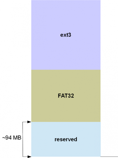
The microSD card provided with BELK/BXELK is partitioned as shown in the following image:
Most of storage space is occupied by two partitions:
- a
FAT32partition (mmcblk0p1) containing:- For BELK <= 3.0.2 and BXELK <= 1.0.1 :
boot.binboot image (containing FSBL, FPGA Bitstream an U-boot binaries)- U-Boot
boot.scrbootscript - Linux kernel and DTB binary images
- For BELK 4.0.0 or newer and BXELK 2.0.0 or newer:
boot.binu-boot SPL imagefpga.bitoptional FPGA bitstreamu-boot.imgu-boot image- U-Boot
boot.scrbootscript - Linux kernel and DTB binary images
- MVM image in OVA format
- For BELK <= 3.0.2 and BXELK <= 1.0.1 :
- an
ext3partition (mmcblk0p2) containing the root file system for the target.
bootscript and root file system are used to boot the target as described in this section.
It is worth remembering that the microSD card is bootable and U-Boot environment is retrieved from (and stored to with saveenv) into the FAT partition as bora.env
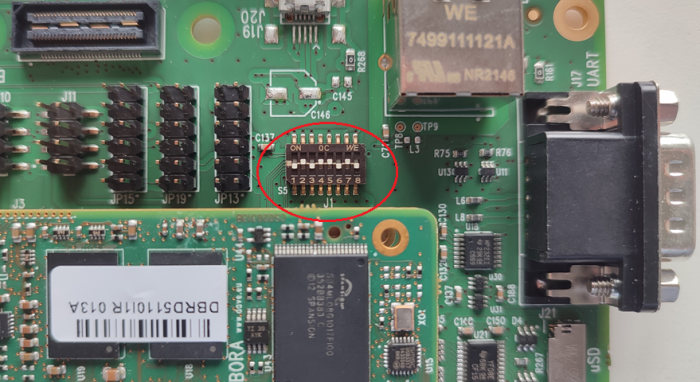
Boot mode selection - S5[edit | edit source]
S5 is a dip-switch for the boot mode selection. The following table reports the available options and the related configurations:
| S5.1 | S5.2 | S5.3 | S5.4 | S5.5 | S5.6 | S5.7 | S5.8 | |
|---|---|---|---|---|---|---|---|---|
| SPI-NOR | OFF | ON | OFF | ON | ON | ON | ON | OFF |
| SD-card | OFF | ON | OFF | ON | ON | OFF | ON | OFF |
| NAND | OFF | ON | OFF | ON | ON | OFF | ON | ON |
| JTAG | OFF | ON | OFF | ON | ON | ON | ON | ON |
Reset Button[edit | edit source]
Reset button - S6[edit | edit source]
S6 is the hardware reset button connected to the MRSTn signal (J2.16 SOM connector)
Carrier board Design[edit | edit source]
Carrier board design guidelines[edit | edit source]
This page provides useful information and resources to system designers in order to design carrier boards hosting DAVE Embedded Systems system-on-modules (SOM).
These guidelines are provided with the goal to help designers to design compliant systems with DAVE Embedded Systems modules and they cover schematics and PCB aspects. They apply to several products that are listed on the top right corner of this page (see "Applies to" boxes).
Basic guidelines[edit | edit source]
In this section basic hardware guidelines valid for all DAVE Embedded Systems SOMs are detailed.
Schematics[edit | edit source]
- Check mirroring and pinout of DAVE Embedded Systems system-on-modules (SOM) connector
- Properly decouple DAVE Embedded Systems system-on-modules (SOM) power supply with large bulk capacitor and small bypass capacitor
- Use low-ESR X7R capacitor if possible
- Check for correct connection of TX and RX lines
- Add series resistors as interface needs (see interface details)
PCB[edit | edit source]
PCB Tecnology[edit | edit source]
Use a PCB technology as advised in the following table
| Parameter | Min | Typ | Max |
| Layers(number) | 4 | 6 | - |
| Power Plane Layers | 2 | 4 | - |
| Clearence(mils) | - | 6 | - |
| Trace Width(mils) | - | 6 | - |
| Vias hole (mechanical) | 0,3 | - | |
| Minimum number of via for each power signal layer changes | 2 | 3 | - |
| Minimum number of via for each power signal SOM connector pin | 1 | 2 | - |
| Component package size | - | 0603 | - |
| PCB Height(mm) | 1,4 | 1,6 | - |
- If vias smaller than minimum advised size are used, take care to maintain an adeguate number of via when you change layer for each power signal.
- PCB heights less than minimum advised can produce PCB heating and mechanical issues
PCB Basics Guidelines[edit | edit source]
- Avoid stubs
- Isolate clock and HI-SPEED signal (see interface specifications for further details)
- Avoid voids on planes
- Use Solid Connection for on plane vias
- Place bulk and ByPass capacitor near DAVE Embedded Systems system-on-modules (SOM) power supply pins
- Place series terminator resistor near the related transmitter
SOM Connectors[edit | edit source]
This section provides information and suggestions regarding the SOM mating connectors.
SO-DIMM[edit | edit source]
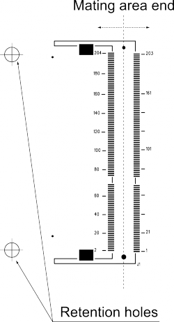
SO-DIMM mating connectors from different vendors may have slight differences in mechanical characteristics. One critical point is the position of the end of the mating area (please see the picture below), that can be slightly shifted inwards or outwards in respect to the retention holes on the carrier board. This can lead to a misalignment with the holes on the SO-DIMM modules, making difficult or impossible to insert the retentions screws or locking supports.
If you plan to use the holes as additional retention system, we recommend to pay attention to the mechanical characteristics when evaluating the SO-DIMM mating connectors to be mounted on the carrier board.
Power-up sequence[edit | edit source]
In order to prevent back powering effects, DAVE Embedded Systems' SOMs provide the signals required to handle power-up sequence properly. For instance, see the recommended sequence for the BORA SOM here.
In case the power-up sequence is not managed properly, the circuitry populating the SOM may be damaged.
Interfaces Guidelines[edit | edit source]
This section provides guidelines for the most used interfaces on DAVE Embedded Systems SOMs module.
Please refer to SOM's detailed pages for specific additional information.
Ethernet 10/100/1000[edit | edit source]
Case #1: PHY is integrated on SOM[edit | edit source]
This section refers to the case of PHY integrated on SOM such as Lizard and MAYA.
Schematics[edit | edit source]
- If LAN connector with integrated magnetic is used:
- predispose ethernet protection diodes on ethernet lines
- Connect connector shield to an adeguate GND or shield Plane
PCB[edit | edit source]
Refer to this table for 10/100 differential pairs routing
| Parameter for 10/100 differential pair | Min | Typ | Max |
| Differential Impedance(ohm) | - | 100 | - |
| Common Mode Impedance | - | 50 | - |
| Gap than TX and RX signals | 2xgap | 2xgap | - |
| Gap than other signals | 2xgap | 4xgap | - |
| Intra pair matching(mils)* | 0 | 25 | 150 |
| TX and RX via # mismatch* | 0 | 0 | 1 |
Refer to this table for Gigabit differential pairs routing
| Parameter for Gigabit Differential Pairs | Min | Typ | Max |
| Differential Impedance(ohm) | - | 100 | - |
| Common Mode Impedance | - | 50 | - |
| Gap than TX and RX signals | 2xgap | 2xgap | - |
| Gap than other signals | 2xgap | 4xgap | - |
| Intra pair matching(mils)* | 0 | 10 | 10 |
| Max PCB trace length | 3" | 5" | - |
| TX and RX via # mismatch* | 0 | 0 | 1 |
* Not mandatory but recommended.
- If LAN connector with integrated magnetic is used:
- do not route traces under the connettor, neither on opposite side
- place filter diode near connector
- place others signals far from connector
- Connect connector shield to an adeguate GND or shield Plane or Copper through numerous vias
- If on board magnetic are used
- adeguately isolate system GND from magnetic connector side
- Connect connector shield to an adeguate GND or shield Plane or Copper through numerous vias if necessary
- try to match as best as possible each differential pair (intrapair matching)
- Keep as best as possibile the same route for TX and RX traces
- If less than minimum gap is used, use a GND trace for improve trace separation
Case #2: PHY is not integrated on SOM and a RGMII PHY is used[edit | edit source]
This section refers to the case of:
- PHY not integrated on SOM
- Gigabit PHY populated on carrier board and connected to SOM through RGMII interface.
This solution is implemented on NaonEVB-Mid for example.
Schematics[edit | edit source]
- Add series resistors (RPACK resistors recommended) to RGMII lines
- Properly decouple PHY Power Supplies rails
- Properly decouple every supply pin of Ethernet PHY
- Properly separate analog Supply Rails
PCB[edit | edit source]
| Parameter for RGMII interface | Min | Typ | Max |
| Common mode impedance(ohm) | - | 50 | - |
| Gap than other ethernet diff pair | 4xwidth | - | - |
| Gap than other signals | 4xwidth | - | |
| Matching(mils) | - | - | 200 |
| Via Mismatch | 0 | 0 | 1 |
| Parameter for Gigabit Differential Pairs | Min | Typ | Max |
| Differential Impedance(ohm) | - | 100 | - |
| Common Mode Impedance | - | 50 | - |
| Gap than TX and RX signals | 2xgap | 2xgap | - |
| Gap than other signals | 2xgap | 4xgap | - |
| Intra pair matching(mils) | 0 | 10 | 10 |
| Max PCB trace length | 3" | 5" | - |
| TX and RX via # mismatch* | 0 | 0 | 1 |
* Not mandatory but recommended.
- Ground and VCC planes must be as large as possible
- Avoid plane split and voids
- Place bypass capacitor near every PHY supply pin
- Connect every capacitor's pin to the plane with at least 2 vias and the shortest trace pattern
- Place PHY device at least 1" (25mm) distance far away from connector
- Keep MDIO clock signal isolated from other signals
Case #3: PHY is not integrated on SOM and a RMII PHY is used[edit | edit source]
This section refers to the case of
- PHY not integrated on SOM
- 10/100 Ethernet PHY populate don carrier board and interfaced to SOM through RMII interface.
This solution is implemented for example in MayaEVB-Lite board.
Schematics[edit | edit source]
- If possible, place series resistor to RMII interface signals
- Properly decouple PHY Power Supplies rails
- Properly separate analog Supply Rails
- Properly decouple every supply pin of Ethernet PHY
- Use a standard RMII PHY that supports correct clock mode (see SOM specification for further details)
PCB[edit | edit source]
| Parameter for RMII interface | Min | Typ | Max |
| Reccomended Common mode impedance(ohm) | - | 50 | - |
| Gap between other signal | 2xW | - |
- Since RMII signals are not critical such as RGMII, is not necessary a strong matching between signal
- Avoid use of long traces
- Avoid stubs
- Keep as best as possibile the same routing for all RMII traces
| Parameter for Ethernet Differential Pairs | Min | Typ | Max |
| Differential Impedance(ohm) | - | 100 | - |
| Common Mode Impedance | - | 50 | - |
| Gap than other TX and RX signals | 2xgap | 2xgap | - |
| Gap than other signals | 2xgap | 4xgap | - |
| Intra pair matching(mils)* | 0 | 25 | 150 |
| TX and RX via # mismatch* | 0 | 0 | 1 |
* Not mandatory but recommended.
- Ground and VCC planes must be as large as possible
- Avoid plane split and voids
- Place bypass capacitor near every PHY supply pin
- Connect every capacitor's pin to the plane with at least 2 vias and the shortest trace pattern
- Place PHY device at least 1" (25mm) distance far away connector
- Keep MDIO clock signal isolated from other signals
USB[edit | edit source]
Schematics[edit | edit source]
- Create schematic in accordance with DAVE Embedded Systems system-on-modules (SOM) USB specification ( see SOM detailed pages )
PCB[edit | edit source]
| Parameter for USB Differential Pairs | Min | Typ | Max |
| Differential Impedance(ohm) | 80 | 90 | 100 |
| Common Mode Impedance | 40,5 | 45 | 49.5 |
| Gap than other signals | 3xgap | 5xgap | - |
| Intra pair matching(mils) | 0 | 25 | 150 |
| Max allowed stubs | - | - | 0 |
| Max traces length | - | - | note 1 |
| Max allowed plane split under traces | - | - | 0 |
note 1 see SOM detailed specifications
- If a stub is unavoidable in the design, no stub should be greater than 200 mils.
- Place a continuos reference plane underneath differential pair
HDMI[edit | edit source]
Schematics[edit | edit source]
- Add a Transmitter Port Protection to HDMI lines
- Use certified HDMI connector
- Connector shield must be properly connected
PCB[edit | edit source]
| Parameter for HDMI Differential Pairs | Min | Typ | Max |
| Differential Impedance(ohm) | 85 | 100 | 115 |
| Gap than other signals | 3xgap | 5xgap | - |
| Intra pair matching(mils) at 225MHz clock | 0 | 20 | 250 |
| Inter pair matching(mils) at 225MHz clock | 0 | 250 | 1" |
| Max allowed stubs | - | - | 0 |
| Max allowed plane split under traces | - | - | 0 |
- Place a continuos reference plane underneath differential pair
- Try to match lines as best as possible
SATA[edit | edit source]
Schematics[edit | edit source]
- Use certified SATA connector
PCB[edit | edit source]
| Parameter for SATA Differential Pairs | Min | Typ | Max |
| Differential Impedance(ohm) | 80 | 100 | 120 |
| Common Mode Impedance(ohm) | 51 | 60 | 69 |
| Gap than other signals | 2xgap | - | - |
| Intra pair matching(mils | - | - | note 1 |
| Inter pair matching(mils) | - | - | note 1 |
| Max allowed stubs | - | - | 0 |
| Max allowed plane split under traces | - | - | 0 |
| Max allowed length | - | - | note 1 |
note 1 see SOM detailed specifications
- Place a continuos reference plane underneath differential pair
- Minimized vias use
- No strong matching required between TX and RX, but keep same route for every differential pair
PCI Express[edit | edit source]
PCB[edit | edit source]
| Parameter for PCI Express Differential Pairs | Min | Typ | Max |
| Differential Impedance [Ohm] | - | 100 | - |
| Common Mode Impedance [Ohm] | - | 60 | - |
| Gap than other signals (reccomended) | - | 2xgap | - |
| Intra pair matching [mils]* | - | - | 10 |
| Max Total Length [in]* | - | - | 12 |
| Maximum allowed stub | - | - | 0 |
| Max allowed vias | - | - | 6 |
- * Including SoM trace length
- Preferred underneath plane over entire trace length GND.
LVDS[edit | edit source]
PCB[edit | edit source]
| Parameter for LVDS Differential Pairs | Min | Typ | Max |
| Differential Impedance [Ohm] | 85 | 100 | 115 |
| Common Mode Impedance [Ohm] | 46.75 | 55 | 63.25 |
| Gap than other signals (reccomended) | - | 2xgap | - |
| Intra pair skew [mils]* | - | - | 5 |
| Inter pair skew [mils]** | - | 400 | - |
| Maximum allowed stub | - | - | 0 |
- Prefer to route traces on TOP layer, referring them to a continuos GND plane.
- * Not includes SOM's length.
- ** Typical value can be relaxed depending on LVDS clock frequency
LCD Interface[edit | edit source]
Schematics[edit | edit source]
- Please refer to DAVE Embedded Systems system-on-modules (SOM) carrier board documentationfor further information
- Predispose series resistor terminator (RPACK for LCD data and single resistor for Clock and H-SYNC and V-SYNC)
- Series resistor value may vary depending by PCB and schematic
PCB[edit | edit source]
- If possible, use 50ohm common mode lines
- Match LCD parallel signals in accordance with Pixel Clock frequency (further details in SOM specifications)
- Avoid use of long traces connection (max 10" on PCB)
- Avoid stubs
VIN Interface[edit | edit source]
Schematics[edit | edit source]
- Please refer to DAVE Embedded Systems system-on-modules (SOM) carrier board documentation for further information
- Predispose series resistor terminator (RPACK for LCD data and single resistor for Clock and H-SYNC and V-SYNC)
- Series resistor value may vary depending PCB and schematic
PCB[edit | edit source]
- If possible, use 50ohm common mode lines
- Match VIN parallel signals in accordance with Pixel Clock frequency (further details in SOM specifications)
- Avoid use of long traces connection (max 10" on PCB)
- Avoid stubs
TVOUT[edit | edit source]
Schematics[edit | edit source]
- Please refer to DAVE Embedded Systems system-on-modules (SOM) carrier board documentation for further information
PCB[edit | edit source]
| Parameter for SATA Differential Pairs | Min | Typ | Max |
| Common Mode Impedance(ohm) | - | 75 | - |
| Gap than other signals | 2xwidth | - | - |
- Keep analog TVOUT signal far from noise signals
I2C Interface[edit | edit source]
Schematics[edit | edit source]
- Predispose properly pullup resistors on line in accordance with DAVE Embedded Systems system-on-modules (SOM)
- Do not overload I2C lines with too much devices
- Ensure that I2C devices are being properly initialized during power up
PCB[edit | edit source]
- Isolate I2C clock from noise sensitive signals
- Avoid stub
SD/MMC Interface[edit | edit source]
| Min | Typ | Max | |
| Common Mode impedance SOM(ohm) | - | 50 | 60 |
| Matching required* | - | - | - |
| Max allowed parallel routing(mils) | - | - | 1000 |
| Max trace Length** | - | - | - |
| Max # of vias allowed | - | - | - |
*This is not mandatory, however it is suggested in case trace length exceeds 10cm
**Overall trace length - i.e. Bora + carrier board - should not exceed 10cm. If this is not possible, try to avoid parallel routing in order to reduce crosstalk, and refer them to a ground plane.
CAN Interface[edit | edit source]
| Min | Typ | Max | |
| Differential Mode impedance(ohm) | 108 | 120 | 132 |
| Matching required | - | - | - |
| Min Interpair spacing | - | 4xgap | - |
| Max allowed parallel routing(mils) | - | - | - |
| Max trace Length | - | - | - |
| Max via allowed | - | - | - |
Functional guidelines[edit | edit source]
Sudden power off management[edit | edit source]
From the architectural standpoint, modern embedded systems often resemble traditional PCs. For example:
- they implement a rich set of I/O interfaces (large displays, Ethernet ports, USB ports, SDIO sockets etc.)
- they likely run complex operating systems that derive from desktop world (linux, Android, Windows CE etc.)
- they implement complex storage schemes (raw NAND, SSD, eMMC etc.).
One of the main difference between such systems and PCs is that the formers are - if appropriately designed - inherently resilient to sudden power fails. In any case, system designer should take into account these events and decide if and how manage them explicitly. Here are some typical techniques used to deal with this situation:
- in case the system is used by human operators, the use of clean shutdown - triggered by the user himself - should be encouraged to prevent sudden power off. Technically speaking, this can be done via GUI (soft button) or mechanical device (push buttons and alike). In the latter case, push button controllers such as Linear LTC2954 can be very useful to implement this feature
- in case no human operators interact with the system, more complex solutions might be required. This strategy is strongly dependent on hardware characteristics of SOM and must be approached on a case-by-case basis.
Thermal Management[edit | edit source]
Heat is generated by all semiconductors while operating and it is dissipated into the surrounding environment. This amount of heat is a function of the power consumed and the thermal resistance of the device package. Every silicon device on an electronic board must work within the limits of its operating temperature parameters (eg, the junction temperature) as specified by the silicon vendor.
Failure to maintain the temperature within safe ranges reduces operating lifetime, reliability, and performances and may cause irreversible damage to the system. Therefore, the product design cycle should include thermal analysis to verify that the device works within its functional limits. If the temperature is too high, component or system-level thermal enhancements are required to dissipate the heat from the system.
For detailed information, please refer to the following documents:
Integration guide[edit | edit source]
This page provides useful information and resources to system designers in order to integrate Bora SoMs in his/her application quickly. These information complement SoM-independent recommendations provided in the Carrier board design guidelines (SOM) page.
Several topics are covered, ranging from hardware issues to manufacturing aspects.
Advanced routing and carrier board design guidelines[edit | edit source]
Generally speaking, when designing a system-on-module (SoM) product it is impossible to know in advance the combination of interfaces and functionalities that will be implemented by the system integrator. This is even more true in case of Bora, due to the unprecedented flexibility and versatility of Zynq architecture. For this reason, Bora implements advanced routing schemes that, in combination with proper carrier board design, allow the implementation of high-speed complex interfaces that satisfy signal integrity requirements.
This chapter describes in detail such schemes and provides carrier board design guidelines accordingly.
In the following section the terms "Inter-pair matching" and "Intra-pair matching" are used. They indicate respectively:
- length matching among pairs belonging to the same class or group
- length matching between traces belonging to the same pair.
Suggested PCB specifications[edit | edit source]
| Min. | Typ. | |
| Layers(number) | 4 | 6 |
| GND Plane Layers | 1 | 2 |
| Power Plane Layers | 1 | 1 |
| Vias hole (mechanical)* [mm] | 0.3 | - |
*Smaller holes are deprecated because their limited current capacity and heat dissipation.
Power rails[edit | edit source]
Following power rails should be kept as short as possible and should be sized in order to minimize IR drop at maximum estimated current.
| Max estimated current | Required plane or copper areas | |
| 3.3V_SOM | application dependent | YES |
| VDDIO_BANK35 | application dependent | NO |
| VDDIO_BANK13 | application dependent | NO |
Main SD/MMC interface[edit | edit source]
Signals: PS_MIO40_501, PS_MIO41_501, PS_MIO42_501, PS_MIO43_501, PS_MIO44_501, PS_MIO45_501.
Following table details routing rules implemented on Bora SoM.
| Value | UOM | |
| Common Mode impedance | 50 | Ohm |
| Maximum Length Tolerance | 200 | mils |
Main Gigabit Ethernet interface (ETH0)[edit | edit source]
Signals: ETH_TXRX0_P/ETH_TXRX0_M, ETH_TXRX1_P/ETH_TXRX1_M, ETH_TXRX2_P/ETH_TXRX2_M, ETH_TXRX3_P/ETH_TXRX3_M.
Following table details routing rules implemented on Bora SoM.
| Value | UOM | |
| Common Mode impedance SOM | 55 | Ohm |
| Differential Mode impedance SOM | 100 | Ohm |
| Maximum Length Tolerance on SOM(intrapair) | 10 | mils |
| Maximum Length Tolerance on SOM(interpair) | 400 | mils |
CAN interface[edit | edit source]
Signals: CAN_H/CAN_L.
Following table details routing rules implemented on Bora SoM.
| Value | UOM | |
| Common Mode impedance SOM | - | Ohm |
| Differential Mode impedance SOM | 110 | Ohm |
| Maximum Length Tolerance on SOM(intrapair) | - | mils |
| Maximum Length Tolerance on SOM(interpair) | - | mils |
XADC interface[edit | edit source]
Signals XADC_VP_R/XADC_VN_R (dedicated analog inputs).
Following table details routing rules implemented on Bora SoM.
| Value | UOM | |
| Differential Mode impedance typ | 100 | Ohm |
| Maximum Length Tolerance on SOM(intrapair) | - | mils |
| Maximum Length Tolerance on SOM(interpair) | - | mils |
| Intrapair Matching required | 10 |
Connecting the PUDC_B pin[edit | edit source]
On Bora SOM, PUDC_B pin is (J2 connector, pin 15) connected to VDDIO_BANK34 (3.3V) via 10K resistor, thus internal pull-up resistors are disabled on each SelectIO pin, until FPGA configuration completes.
Default behavior can be changed by appropriate circuitry at carrier board level to set it to logical 0.
PS' I²C buses[edit | edit source]
Xilinx released an important Answer Record related to Zynq PS I2C Controller on 19th September 2014 (http://www.xilinx.com/support/answers/61861.html), a long period after Bora public lunch.
A technical and functional assessment has been performed to find out the best solution to cope with this issue on Bora based systems (1). Bora SoM is conceived to address a wide range of different application environments that are by definition unknown at design stage. Therefore it is virtually impossible to find a one-size-fits-all solution that does not limit somehow Bora functionalities and is backward compatible. The followed approach has aimed to preserve:
- system reliability
- backward compatibility
- system designer's freedom to choose the appropriate solution for his/her specific application.
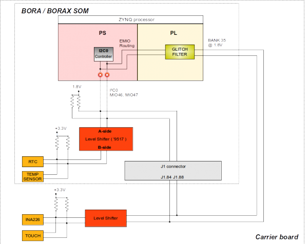
Thanks to the Bora's I2C0 topology, Bora has undergone no changes to satisfy these requirements. The SoM in fact allows for:
- implementing, at carrier board level, complex glitch filtering strategies such as the one suggested by Xilinx AR# 61861
- avoiding waste of resources of PL if not strictly necessary (for instance when I2C0 functionality is not required at all).
The configuration depicted by the following figure shows in principle a solution integrating the workaround suggested by Xilinx AR# 61861:
- PS I2C0 controller's signals are routed to PL via EMIO routing
- MIO46/47 are disabled
- glitch filter is digitally implemented in PL
- I2C0 SDA and SCL lines are physically connected to PL at carrier board level.
(1) What here described refers to I2C0 controller that by default is routed on pins MIO46 and MIO47.
How to implement workaround suggested by Xilinx on BoraEVB[edit | edit source]
Plase note that the reference project with I2C glitch filter implemented in FPGA is available on request. Plase contact helpdesk@dave.eu
This project, built with Vivado 2014.4, is based on the default project for BELK (BORA rev.B and BORAevb rev.A).
Here we have changed I2C0 signals routing to EMIO pins through FPGA, implementing the I2C glitch filter with VHDL example code provided in Xilinx AR# 61861. The MIO46-MIO47 is then configured as input GPIO. This is accomplished from the FSBL generated within the provided project.
I2C interface is routed through FPGA to pins on BANK35:
- I2C SCL => IO_L9P_T1_DQS_AD3P_35
- I2C SDA => IO_L9N_T1_DQS_AD3N_35
The BANK35 MUST be powered at 1.8V
Test on BoraEVB[edit | edit source]
To test the solution, please make these connections on BORAevb rev.A:
- 1.8V supply for BANK35 : (J11.2 to J11.7)
- I2C SCL : JP10.14 to JP21.5
- I2C SDA : JP10.16 to JP21.3
Test on BoraXEVB[edit | edit source]
To test the solution, please make these connections on BoraXEVB:
- 1.8V supply for BANK35 : please refer to VDDIO_BANK35 possibility on BoraXEVB schematics
- populate RPACK RP87
- I2C SCL : JP30.9 to JP29.5
- I2C SDA : JP30.11 to JP29.3
Programmable logic (PL)[edit | edit source]
For Bora SOM please refer to the following links:
For BoraX SOM please refer to the page.
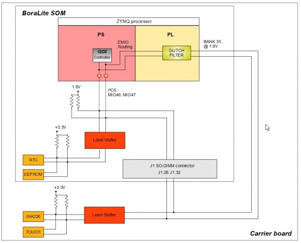
For BoraLite SOM please refer to the page.
Traces length matching[edit | edit source]
A spreadsheet is available for download here, containing detailed information about signals routing. These information can be used to check nets matching of the overall system (carrier board + SOM).
For Bora/BoraEVB systems: File:Bora-routing.zip.
For BoraX/BoraXEVB systems: File:BoraX-BoraXEVB-combined-routing.zip.
For BoraLite/BoraXEVB systems: the presence of the Bora Lite adapter does not make sense to provide the routing information. Please refer to the Programmable logic page about information on internal BORA Lite routing. Please take carefully into account the design of the Carrier board considering every information related to the SO-DIMM socket and the tracenet on the Carrier
General Information[edit | edit source]
Product Highlights[edit | edit source]
The BORA Evaluation platform presented here provides a compact solution for any industry and can be easily interfaced with Digital signal Processing application, Plant Automation Control thanks to IEC-61131 SW language environment and/or other GUI QT framework.
The following table summarizes the main hardware and software features available with BORA EVB:
Hardware[edit | edit source]
| Subsystem | Characteristics |
|---|---|
| CPU | Zynq 7000 Dual Core Cortex-A9 |
| SD | microSD boot device |
| USB | OTG |
| Serial Ports | RS232 CAN interface |
| Ethernet0 | Dual EMAC 10/100/1000Mbps |
| Ethernet1 | Dual EMAC 10/100/1000Mbps (routed through EMIO) |
| Memory | External DDR3 SDRAM bank |
| Display | LVDS interface |
| Touchscreen | Resistive |
| Espansion | GPIO connector Digilent Pmod™ Compatible connector |
| WiFi | Socket for DWM Wireless Module |
| JTAG | JTAG and TRACE ports |
| PSU | 12 to 24V DC |
Software[edit | edit source]
| Subsystem | Options |
|---|---|
| Operating System | Linux |
| Distribution | Yocto, Petalinux |
| Applications | SoftPLC |
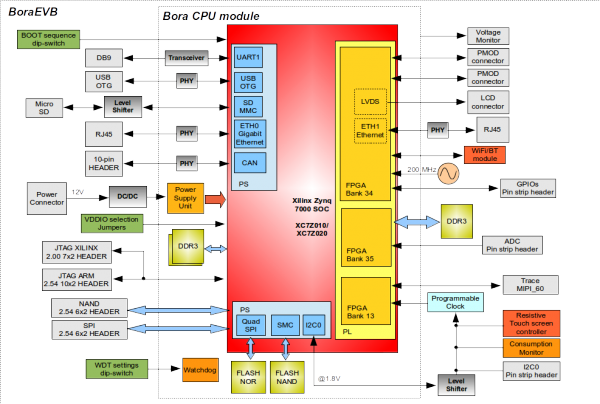
Block Diagram[edit | edit source]
The following picture shows BoraEVB block diagram:
Interfaces and Connectors[edit | edit source]
Power Supply[edit | edit source]
Power supply - J7[edit | edit source]
Power is provided through the J7 connector.
| Pin# | Pin name | Function | Notes |
|---|---|---|---|
| 1 | VIN | Power supply | Nominal: +12V |
| 2 | DGND | Ground | - |
POWER GOOD signals selector - J10[edit | edit source]
J10 is a 8-pin 4x2x2.54 pitch vertical header used for the selection - through jumpers - of the POWER GOOD options. The following table reports the pinout of the connector:
| Pin# | Pin name | Function | Notes |
|---|---|---|---|
| 1 | BOARD_PGOOD | - | - |
| 2, 4 | 3.3V_SOM | - | - |
| 3 | 1.5V_POWER_GOOD | - | - |
| 5 | VREF_POWER_GOOD | - | - |
| 6, 8 | 3.3V_SBY | - | - |
| 7 | 1.8V_POWER_GOOD | - | - |
The available configurations are:
- No jumpers mounted (DEFAULT)
- Jumper on 1-2 -> supply BOARD_PGOOD with 3.3V_SOM
- Jumper on 3-4 -> supply 1.5V_POWER_GOOD with 3.3V_SOM
- Jumper on 5-6 -> supply 1.5V_VREF_POWER_GOOD with 3.3V_SBY
- Jumper on 7-8 -> supply 1.8V_VREF_POWER_GOOD with 3.3V_SBY
BANK35, BANK13 VDDIO selector - J11[edit | edit source]
J11 is a 8-pin 4x2x2.54 pitch vertical header used for the selection - through jumpers - of the bank supply voltages. The following table reports the pinout of the connector:
| Pin# | Pin name | Function | Notes |
|---|---|---|---|
| 1, 5 | 3.3V | - | - |
| 2, 4 | VDDIO_BANK35 | - | - |
| 3 | EVB_VDDQ_1V5 | - | - |
| 6, 8 | VDDIO_BANK13 | - | - |
| 7 | EVB_VDDIO_BANK13 | - | - |
The available configurations are:
- Jumper on 1-2 -> supply VDDIO_BANK35 with 3.3V (requirerd when EVBB DDR3 device is used)
- Jumper on 3-4 -> (Not Available) supply VDDIO_BANK35 with EVB_VDDQ_1V5 (requirerd when EVBB DDR3 device is used)
- Jumper on 5-6 -> supply VDDIO_BANK13 with 3.3V
- Jumper on 7-8 -> supply VDDIO_BANK13 with EVB_VDDIO_BANK13 (requirerd when TRACE is used)
The following rules must be observed:
- Because of a hardware limitation, VDDIO_BANK35 must be configured for 3.3V power supply (Jumper on 1-2).
- The configuration 1. (Jumper on 1-2) excludes 2. (Jumper on 3-4) (and viceversa)
- The configuration 3. (Jumper on 5-6) excludes 4. (Jumper on 7-8) (and viceversa)
The DEFAULT configuration is:
- Jumper on 1-2 (please note that this jumper must not be removed)
- Jumper on 5-6
CPU connectors[edit | edit source]
J1,J2 and J3[edit | edit source]
The pinout of the J1, J2 and J3 connectors of the Bora EVB is the same of the counterpart connectors on BORA module.
JTAG[edit | edit source]
JTAG[edit | edit source]
JTAG port is available as two different mechanical connectors:
- 2.00mm-pitch 7x2 header (Xilinx standard)
- 2.54mm-pitch 10x2 header (ARM standard): http://www2.lauterbach.com/pdf/arm_app_jtag.pdf
- This port is connected to Zynq's native JTAG signals. Please note that Zynq's internal JTAG chain supports differents configurations, depending on bootstrap signals. In case split mode is selected, CPU JTAG can be routed separately via PL. For more details please refer to Zynq Technical Reference Manual.
JTAG XILINX - J13[edit | edit source]
J13 is a 14-pin 7x2x2 pitch vertical header. The following table reports the pinout of the connector:
| Pin# | Pin name | Function | Notes |
|---|---|---|---|
| 1, 3, 5, 7, 9, 11, 13 | DGND | - | - |
| 2 | 3.3V | - | - |
| 4 | JTAG_TMS | - | - |
| 6 | JTAG_TCK | - | - |
| 8 | JTAG_TDO | - | - |
| 10 | JTAG_TDI | - | - |
| 12 | N.C. | - | - |
| 14 | JTAG_TRSTn | - | - |
JTAG ARM - J18[edit | edit source]
J18 is a 20-pin 10x2x2.54 pitch vertical header. The following table reports the pinout of the connector:
| Pin# | Pin name | Function | Notes |
|---|---|---|---|
| 1 | 3.3V | - | - |
| 2 | 3.3V | - | - |
| 3, 11, 17, 19 | N.C. | - | - |
| 4, 6 ,8 ,10 ,12, 14, 16, 18, 20 |
DGND | - | - |
| 5 | JTAG_TDI | - | - |
| 7 | JTAG_TMS | - | - |
| 9 | JTAG_TCK | - | - |
| 13 | JTAG_TDO | - | - |
| 15 | JTAG_TRSTn | - | - |
TRACE[edit | edit source]
Trace Port - J22[edit | edit source]
J22 is a QSH–060–01–L–D–A 0,50 mm Hi-speed socket. It is connected to the Debug Trace Port. From the physical standpoint, trace port exploits the advanced routing of bank 13 signals implemented on Bora, combined with the possibility to select the I/O voltage of bank itself. Connector is compatible with ETMv1/ETMv3 specification. Please refer to http://www.lauterbach.com/frames.html?adetmmipi60.html for more details.
Please note that:
- JTAG and trace signals are EMIO routed to I/O of bank 13
- About tracing, several differents schemes are possible, depending of debug requirements. For example one might be interested in CPU-only tracing via PTM or fabric-only tracing via FTM. For more details please refer to Zynq TRM and these links:
The following table reports the pinout of the connector:
| Pin# | Pin name | Function | Notes |
|---|---|---|---|
| 1 | 3.3V | - | - |
| 2 | JTAG_TMS | - | - |
| 3 | JTAG_TCK | - | - |
| 4 | JTAG_TDO | - | - |
| 5 | JTAG_TDI | - | - |
| 6 | JTAG_TRSTn | - | - |
| 7, 8, 9, 10, 11, 18, 20, 22, 24 ,26, 28, 30, 32, 34, 36, 38, 40 |
N.C. | - | - |
| 12 | VDDIO_BANK13 | - | - |
| 13 | IO_L15N_T2_DQS_13 | - | - |
| 14, 15, 16, ,42, 44, 46, 48, 50, 52, 54, 56, 57, 58, 59, 60 |
DGND | - | - |
| 17 | IO_L15P_T2_DQS_13 | - | - |
| 19 | IO_L17N_T2_13 | - | - |
| 21 | IO_L17P_T2_13 | - | - |
| 23 | IO_L20N_T3_13 | - | - |
| 25 | IO_L20P_T3_13 | - | - |
| 27 | IO_L22N_T3_13 | - | - |
| 29 | IO_L22P_T3_13 | - | - |
| 31 | IO_L6N_T0_VREF_13 | - | - |
| 33 | IO_L12N_T1_MRCC_13 | - | - |
| 35 | IO_L12P_T1_MRCC_13 | - | - |
| 37 | IO_L14N_T2_SRCC_13 | - | - |
| 39 | IO_L14P_T2_SRCC_13 | - | - |
| 41 | IO_L16N_T2_13 | - | - |
| 43 | IO_L16P_T2_13 | - | - |
| 45 | IO_L18N_T2_13 | - | - |
| 47 | IO_L18P_T2_13 | - | - |
| 49 | IO_L19N_T3_VREF_13 | - | - |
| 51 | IO_L19P_T3_13 | - | - |
| 53 | IO_L21N_T3_DQS_13 | - | - |
| 55 | IO_L21P_T3_DQS_13 | - | - |
| 61, 62, 63, 64 | DGND | - | - |
Ethernet[edit | edit source]
Ethernet port #0 (ETH0) - J8[edit | edit source]
J8 is a RJ45 Gigabit Ethernet connector - incorporating magnetics - connected to the Bora integrated ethernet controller and PHY.
| Pin# | Pin name | Function | Notes |
|---|---|---|---|
| 1 | ETH_TXRX0_P | - | - |
| 2 | ETH_TXRX0_M | - | - |
| 3 | ETH_TXRX1_P | - | - |
| 4 | ETH_TXRX2_P | - | - |
| 5 | ETH_TXRX2_M | - | - |
| 6 | ETH_TXRX1_M | - | - |
| 7 | ETH_TXRX3_P | - | - |
| 8 | ETH_TXRX3_M | - | - |
| 9 | 3.3V_ETH0 | - | - |
| 10 | GND_ETH0 | - | - |
| 11, 13 | +3.3V | - | - |
| 12 | 3.3V_ETH0_LED1 | - | - |
| 14 | 3.3V_ETH0_LED2 | - | - |
Ethernet port #1 (ETH1) - J9[edit | edit source]
J9 is a RJ45 Gigabit Ethernet connector - incorporating magnetics - connected to Micrel KSZ9031 PHY (Gigabit Ethernet Transceiver). This, in turn, is connected to PL's bank 34 via RGMII interface. This is an example of EMIO routing showing how to route PS's MAC signals via PL subsystem. Please note that, in case PL is not properly configured, this second Ethernet port will not work.
| Pin# | Pin name | Function | Notes |
|---|---|---|---|
| 1 | ETH1_TXRX0_P | - | - |
| 2 | ETH1_TXRX0_M | - | - |
| 3 | ETH_TXRX1_P | - | - |
| 4 | ETH1_TXRX2_P | - | - |
| 5 | ETH1_TXRX2_M | - | - |
| 6 | ETH1_TXRX1_M | - | - |
| 7 | ETH1_TXRX3_P | - | - |
| 8 | ETH1_TXRX3_M | - | - |
| 9 | 3.3V_ETH1 | - | - |
| 10 | GND_ETH1 | - | - |
| 11, 13 | +3.3V | - | - |
| 12 | 3.3V_ETH1_LED1 | - | - |
| 14 | 3.3V_ETH1_LED2 | - | - |
Console[edit | edit source]
UART1 - J17[edit | edit source]
J17 is a standard DB9 connector that routes the signals coming from the RS232 transceiver that is connected to the PS MIO signals of the UART1 port.
| Pin# | Pin name | Function | Notes |
|---|---|---|---|
| 1, 6, 4, 9 | N.C. | N.C. | |
| 2 | UART_EXT_RX | Receive line | Connected to protection diode array |
| 3 | UART_EXT_TX | Transmit line | Connected to protection diode array |
| 5 | DGND | Ground | |
| 7, 8 | N.C. | N.C. | Connected to protection diode array |
SD[edit | edit source]
MicroSD - J21[edit | edit source]
J21 is a microSD memory card connector. It is connected to the Bora SOM through a bidirectional 1.8V/3.3V voltage-level translator mounted on the BoraEVB. Level shifter is required because MIO signals are 1.8V. The following table reports the pinout of the connector:
| Pin# | Pin name | Function | Notes |
|---|---|---|---|
| 1 | PS_SD0_DAT2 | - | - |
| 2 | PS_SD0_DAT3 | - | - |
| 3 | PS_SD0_CMD | - | - |
| 4 | 3.3V | - | - |
| 5 | PS_SD0_CLK | - | - |
| 6, 9, 10, 11, 12 | DGND | - | - |
| 7 | PS_SD0_DAT0 | - | - |
| 8 | PS_SD0_DAT1 | - | - |
| 3.3V | - | Pull up to 3.3V with 10K Ohm - |
USB[edit | edit source]
USB OTG - J19[edit | edit source]
J19 is a standard USB MICRO AB connector. It is connected to the Bora USB 2.0 OTG peripheral. The following table reports the pinout of the connector:
| Pin# | Pin name | Function | Notes |
|---|---|---|---|
| 1 | USB_OTG_VBUS | - | - |
| 2 | USBM1 | - | - |
| 3 | USBP1 | - | - |
| 4 | OTG_ID | - | - |
| 5 | USB_OTG_DGND | - | - |
| 6, 7, 8, 9 | USB_OTG_SHIELD | - | - |
LVDS[edit | edit source]
LVDS - J26[edit | edit source]
J26 is a vertical double row straight 20-pin 1.25mm pitch header. This interface shows how to implement a differential connection to an LCD screen. As known, Zynq does not implement an LCD controller, however this can be integrated in FPGA fabric as shown by this example: https://wiki.analog.com/resources/tools-software/linux-drivers/platforms/zynq. The following table reports the pinout of the connector:
| Pin# | Pin name | Function | Notes |
|---|---|---|---|
| 1, 2 | 3.3V_LCD | - | - |
| 3, 4, 7, 10, 13, 16, 19 |
DGND | Ground | - |
| 5 | LCD_LVDS_D0- | - | - |
| 6 | LCD_LVDS_D0+ | - | - |
| 8 | LCD_LVDS_D1- | - | - |
| 9 | LCD_LVDS_D1+ | - | - |
| 11 | LCD_LVDS_D2- | - | - |
| 12 | LCD_LVDS_D2+ | - | - |
| 15 | LCD_LVDS_CLK+ | - | - |
| 17 | LCD_P17 | - | - |
| 18 | LCD_P18 | - | - |
| 20 | LCD_P20 | - | - |
| 21,22 | DGND | Ground | Shield |
Touchscreen[edit | edit source]
Touch screen - J25[edit | edit source]
J25 is a ZIF 4-pin 1.0mm pitch connector that connects the touchscreen drive lines to the touch screen controller on the BoraEVB. The following table reports the pinout of the connector:
| Pin# | Pin name | Function | Notes |
|---|---|---|---|
| 1 | TSC_YP | - | - |
| 2 | TSC_XP | - | - |
| 3 | TSC_YM | - | - |
| 4 | TSC_XM | - | - |
CAN[edit | edit source]
CAN - J24[edit | edit source]
J24 is a 10-pin 5x2x2.54mm pitch vertical header directly connected to Bora SoM's transceiver for the CAN interface. This 2.5mm-pitch header is compatible with commonly available IDC-10/DB9 flat cables. The following table reports the pinout of the connector:
| Pin# | Pin name | Function | Notes |
|---|---|---|---|
| 1, 6, 7, 8, 9, 10 |
N.C. | - | - |
| 2, 5 | CAN_SHIELD | - | - |
| 3 | CAN_L | - | - |
| 4 | CAN_H | - | - |
RTC[edit | edit source]
FPGA, WatchDog, RTC, RST - JP22[edit | edit source]
JP22 is a 16-pin 8x2x2.54 pitch vertical header. The following table reports the pinout of the connector:
| Pin# | Pin name | Function | Notes |
|---|---|---|---|
| 1 | FPGA_INIT_B | - | - |
| 2 | RTC_32KHZ | - | - |
| 3 | FPGA_PROGRAM_B | - | - |
| 4 | RTC_RST | - | - |
| 5 | FPGA_DONE | - | - |
| 6 | RTC_INT/SQW | - | - |
| 7, 8 | DGND | Ground | - |
| 9 | WD_SET0 | - | - |
| 10 | SYS_RSTn | - | - |
| 11 | WD_SET1 | - | - |
| 12 | PORSTn | - | - |
| 13 | WD_SET2 | - | - |
| 14 | MRSTn | - | - |
| 15 | PS_MIO15_500 | - | - |
| 16 | CB_PWR_GOOD | - | - |
Watchdog[edit | edit source]
WatchDog Settings - S1, S2 and S3[edit | edit source]
S1, S2 and S3 are dip-switch to override the default startup delay and timeout of the Bora module watchdog. For more details please refer to this page.
| S1.1 | S1.2 | |
|---|---|---|
| WD_SET0 SOM default | OFF | OFF |
| WD_SET0 = '1' | ON | OFF |
| WD_SET0 = '0' | OFF | ON |
| S2.1 | S2.2 | |
|---|---|---|
| WD_SET1 SOM default | OFF | OFF |
| WD_SET1 = '1' | ON | OFF |
| WD_SET1 = '0' | OFF | ON |
| S3.1 | S3.2 | |
|---|---|---|
| WD_SET2 SOM default | OFF | OFF |
| WD_SET2 = '1' | ON | OFF |
| WD_SET2 = '0' | OFF | ON |
DWM[edit | edit source]
DWM (DAVE Wifi/BT module) socket - J23[edit | edit source]
J23 is a 52991-0308 connector type (30 pins, vertical, 0.50mm picth). This socket connects the DWM Wireless Module (optional) to the BoraEVB. The following table reports the pinout of the connector:
| Pin# | Pin name | Function | Notes |
|---|---|---|---|
| 1, 2 | 5V | - | - |
| 3, 4 | 3.3V | - | - |
| 5, 6, 9, 10, 19 |
DGND | - | - |
| 7 | DWM_SD_CMD | - | - |
| 8 | DWM_SD_CLK | - | - |
| 11 | DWM_SD_DAT0 | - | - |
| 12, 14, 16, 18, 20, 22 |
N.C. | - | - |
| 13 | DWM_SD_DAT1 | - | - |
| 15 | DWM_SD_DAT2 | - | - |
| 17 | DWM_SD_DAT3 | - | - |
| 21 | DWM_UART_RX | - | - |
| 23 | DWM_UART_CTS | - | - |
| 24 | DWM_BT_F5 | - | - |
| 25 | DWM_UART_TX | - | - |
| 26 | DWM_BT_F2 | - | - |
| 27 | DWM_UART_RTS | - | - |
| 28 | DWM_WIFI_IRQ | - | - |
| 29 | DWM_BT_EN | - | - |
| 30 | DWM_WIFI_EN | - | - |
PMOD[edit | edit source]
Digilent Pmod™ Compatible headers[edit | edit source]
Please note that:
- Digilent Pmod™ Interface Specification - defined by Digilent Inc. - allows to quickly connect several pre-built I/O modules to PL:
- Signals used to implement LVDS LCD interface can alternatively routed to Digilent Pmod™ Compatible compatible connector
Digilent Pmod™ Compatible - JP17[edit | edit source]
JP17 is a 12-pin 6x2x2.54 pitch vertical header. The following table reports the pinout of the connector:
| Pin# | Pin name | Function | Notes |
|---|---|---|---|
| 1 | PMOD_A0 | - | |
| 2 | PMOD_A4 | - | |
| 3 | PMOD_A1 | - | |
| 4 | PMOD_A5 | - | |
| 5 | PMOD_A2 | - | |
| 6 | PMOD_A6 | - | |
| 7 | PMOD_A3 | - | |
| 8 | PMOD_A7 | - | |
| 9, 10 | DGND | Ground | - |
| 11, 12 | 3.3V | - |
Digilent Pmod™ Compatible - JP23[edit | edit source]
JP23 is a 12-pin 6x2x2.54 pitch vertical header. The following table reports the pinout of the connector:
| Pin# | Pin name | Function | Notes |
|---|---|---|---|
| 1 | PMOD_B0 | - | - |
| 2 | PMOD_B4 | - | - |
| 3 | PMOD_B1 | - | - |
| 4 | PMOD_B5 | - | - |
| 5 | PMOD_B2 | - | - |
| 6 | PMOD_B6 | - | - |
| 7 | PMOD_B3 | - | - |
| 8 | PMOD_B7 | - | - |
| 9, 10 | DGND | Ground | - |
| 11, 12 | 3.3V | - | - |
Pin strip[edit | edit source]
Pin strip connectors[edit | edit source]
ADC - JP10[edit | edit source]
JP10 is a 16-pin 8x2x2.54 pitch vertical header. The following table reports the pinout of the connector:
| Pin# | Pin name | Function | Notes |
|---|---|---|---|
| 1 | IO_0_35 | - | - |
| 2, 4 | VDDIO_BANK35 | - | - |
| 3, 6, 9, 12, 15 | XADC_GND | - | - |
| 5 | ZYNQ_AD14P_35 | - | Mount option |
| 7 | ZYNQ_AD14N_35 | - | Mount option |
| 8 | ZYNQ_T0_VREF_35 | - | Mount option |
| 10 | ZYNQ_T3_VREF_35 | - | Mount option |
| 11 | ZYNQ_AD1P_35 | - | Mount option |
| 13 | ZYNQ_AD1N_35 | - | Mount option |
| 14 | ZYNQ_AD3P_35 | - | Mount option |
| 16 | ZYNQ_AD3N_35 | - | Mount option |
SPI,NAND - JP13[edit | edit source]
JP13 is a 12-pin 6x2x2.54 pitch vertical header. The following table reports the pinout of the connector:
| Pin# | Pin name | Function | Notes |
|---|---|---|---|
| 1, 4, 9, 12 | DGND | Ground | - |
| 2 | SPI0_CS0n | - | - |
| 3 | ZYNQ_SPI0_SCLK/NAND_IO1 | - | - |
| 5 | ZYNQ_SPI0_DQ0/NAND_ALE | - | - |
| 6 | NAND_CS0/SPI0_CS1 | - | - |
| 7 | ZYNQ_SPI0_DQ2/NAND_IO2 | - | - |
| 8 | ZYNQ_SPI0_DQ1/NAND_WE | - | - |
| 10 | ZYNQ_SPI0_DQ3/NAND_IO0 | - | - |
| 11 | ZYNQ_NAND_RD_B | - | - |
Voltage Monitor - JP15[edit | edit source]
JP15 is a 12-pin 6x2x2.00 pitch vertical header. The following table reports the pinout of the connector:
| Pin# | Pin name | Function | Notes |
|---|---|---|---|
| 1 | MON_VCCPLL | - | - |
| 2 | MON_3.3V | - | - |
| 3 | MON_XADC_VCC | - | - |
| 4 | MON_1V2_ETH | - | - |
| 5 | MON_FPGA_VDDIO_BANK35 | - | - |
| 6 | MON_VDDQ_1V5 | - | - |
| 7 | MON_FPGA_VDDIO_BANK34 | - | - |
| 8 | MON_1.8V | - | - |
| 9 | MON_FPGA_VDDIO_BANK13 | - | - |
| 10 | MON_1.0V | - | - |
| 11 | MON_1.8V_IO | - | - |
| 12 | DGND | Ground | - |
Ethernet GPIO - JP18[edit | edit source]
JP18 is a 12-pin 6x2x2.54 pitch vertical header. The following table reports the pinout of the connector:
| Pin# | Pin name | Function | Notes |
|---|---|---|---|
| 1, 2, 5, 6, 16 |
DGND | Ground | - |
| 3 | CLK125_NDO | - | - |
| 4 | ETH1_CLK125_NDO | - | - |
| 7 | ETH_MDC | - | - |
| 8 | ETH1_MDC | - | - |
| 9 | ETH_MDIO | - | - |
| 10 | ETH1_MDIO | - | - |
| 11 | ETH_INTn | - | - |
| 12 | ETH1_INTn | - | - |
| 13 | PS_MIO51_501 | - | - |
| 14 | ETH1_RESETn | - | - |
| 15 | PS_MIO50_501 | - | - |
SPI,NAND - JP19[edit | edit source]
JP19 is a 16-pin 8x2x2.54 pitch vertical header. The following table reports the pinout of the connector:
| Pin# | Pin name | Function | Notes |
|---|---|---|---|
| 1, 11, 12 | DGND | Ground | - |
| 2 | NAND_BUSY | - | - |
| 3 | ZYNQ_NAND_CLE | - | - |
| 4 | NAND_IO3 | - | - |
| 5 | NAND_IO4 | - | - |
| 6 | NAND_IO5 | - | - |
| 7 | NAND_IO6 | - | - |
| 8 | NAND_IO7 | - | - |
| 9 | CONN_SPI_RSTn | - | - |
| 10 | MEM_WPn | - | - |
ADC - JP20[edit | edit source]
JP20 is a 12-pin 6x2x2.54 pitch vertical header. The following table reports the pinout of the connector:
| Pin# | Pin name | Function | Notes |
|---|---|---|---|
| 1 | VDDIO_BANK35 | - | - |
| 2, 6, 11, 12 |
XADC_AGND | - | - |
| 3 | ZYNQ_AD0P_35 | - | - |
| 4 | MON_XADC_VCC | - | - |
| 5 | ZYNQ_AD15P_35 | - | - |
| 7 | ZYNQ_AD15N_35 | - | - |
| 8 | XADC_VN_R | - | - |
| 9 | ZYNQ_AD2P_35 | - | - |
| 10 | XADC_VP_R | - | - |
I2C, BANK34 - JP21[edit | edit source]
JP21 is a 16-pin 8x2x2.54 pitch vertical header. The following table reports the pinout of the connector:
| Pin# | Pin name | Function | Notes |
|---|---|---|---|
| 1 | EVB_1.8V | - | - |
| 2 | 3.3V | - | - |
| 3 | PS_I2C0_DAT | - | - |
| 4 | I2C0_SDA | - | - |
| 5 | PS_I2C0_CK | - | - |
| 6 | I2C0_SCL | - | - |
| 7, 8, 12, 13 |
DGND | Ground | - |
| 9 | IO_L6P_T0_34 | CAN Transmitter | - |
| 10 | INA_ALERT | - | - |
| 11 | IO_L19P_T3_34 | CAN Receiver | - |
| 14 | IO_L3P_T0_DQS_PUDC_B_34 | - | - |
| 15 | IO_25_34 | - | - |
| 16 | IO_0_34 | - | - |
Please note that:
- Three devices are connected to I2C0 bus (this is level shifted from 1.8V to 3.3V):
- Silicon Labs Si571 programmable clock generator: this clock si connected to PL to allow the user to easily experiment his/her own peripherals and IPs on FPGA
- resistive touch screen controller for LCD screen
- consumption monitor: this is connected to shunt resistor put in series on Bora power rail, allowing to measure SoM consumption
FPGA, WatchDog, RTC, RST - JP22[edit | edit source]
JP22 is a 16-pin 8x2x2.54 pitch vertical header. The following table reports the pinout of the connector:
| Pin# | Pin name | Function | Notes |
|---|---|---|---|
| 1 | FPGA_INIT_B | - | - |
| 2 | RTC_32KHZ | - | - |
| 3 | FPGA_PROGRAM_B | - | - |
| 4 | RTC_RST | - | - |
| 5 | FPGA_DONE | - | - |
| 6 | RTC_INT/SQW | - | - |
| 7, 8 | DGND | Ground | - |
| 9 | WD_SET0 | - | - |
| 10 | SYS_RSTn | - | - |
| 11 | WD_SET1 | - | - |
| 12 | PORSTn | - | - |
| 13 | WD_SET2 | - | - |
| 14 | MRSTn | - | - |
| 15 | PS_MIO15_500 | - | - |
| 16 | CB_PWR_GOOD | - | - |
Electrical and Mechanical Documents[edit | edit source]
Schematics[edit | edit source]
|
The following list details the schematic version/serial number association. For more details about the serial number composition, please refer to this page. The following serial numbers were manufactured according to the schematics version 2.4.0:
The following serial numbers were manufactured according to the schematics version 2.2.0:
|
|
U14 DDR3 chip can be populated alternatively with Micron MT41K64M16JT-15E or ISSI IS43TR16256BL-125KBLI |
Release 2.4.0[edit | edit source]
Release 2.2.1[edit | edit source]
BOM[edit | edit source]
|
The following list details the BOM version/serial number association. For more details about the serial number composition, please refer to this page. The following serial numbers were manufactured according to the BOM version 2.4.0:
The following serial numbers were manufactured according to the BOM version 2.2.0:
|
Release 2.4.0[edit | edit source]
- BoraEVB: BORAEVB_S.EVBB0000I1R.2.4.0.CSV.zip
Release 2.2.0[edit | edit source]
Layout[edit | edit source]
