AXEL Lite SOM/AXEL Lite Hardware/pdf
General Information[edit | edit source]
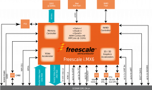
AXEL Lite Block Diagram[edit | edit source]
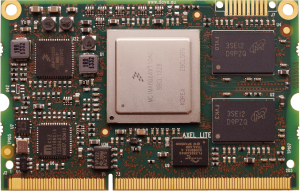
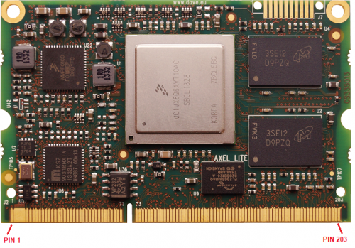
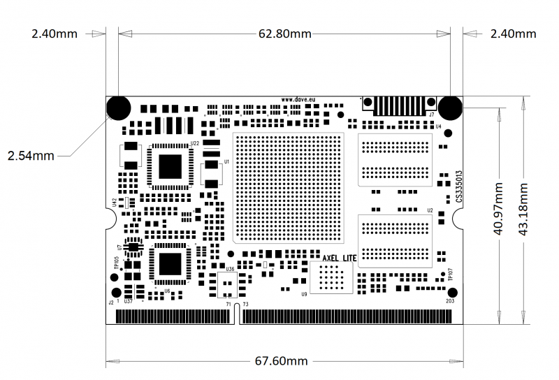
AXEL Lite TOP View[edit | edit source]
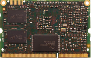
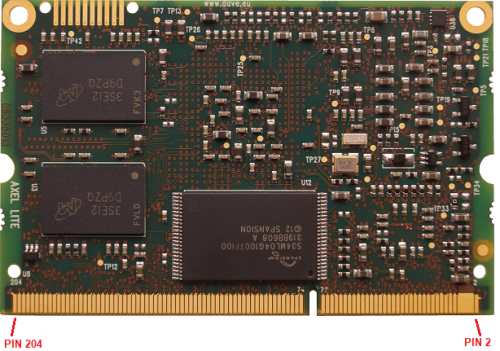
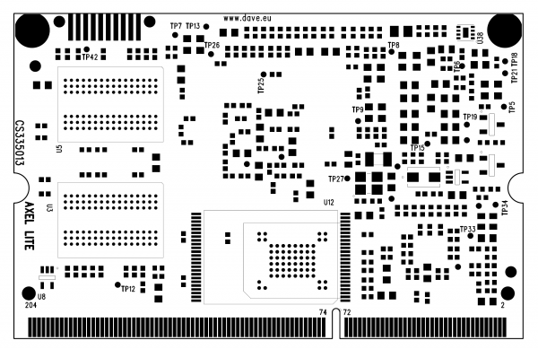
AXEL Lite BOTTOM View[edit | edit source]
Processor and memory subsystem[edit | edit source]
The heart of AXEL Lite module is composed by the following components:
- i.MX6 SoC application processor
- Power supply unit
- DDR memory banks
- NOR and NAND flash banks
- SO-DIM 204 pin connector with interfaces signals
This chapter shortly describes the main Axel Lite components.
Processor Info[edit | edit source]
| Processor | # Cores | Clock | L2 Cache | DDR3 | Graphics Acceleration | IPU | VPU | SATA-II |
| i.MX6 Solo | 1 | 800 MHz 1 GHz |
512 KB | 32 bit @ 400 MHz | 3D: Vivante GC880 2D: Vivante GC320 Vector: N.A. |
1x | 1x | No |
| i.MX6 DualLite | 2 | 850 MHz 1 GHz |
512 KB | 64 bit @ 533 MHz | 3D: Vivante GC880 2D: Vivante GC320 |
1x | 1x | No |
| i.MX6 Dual | 2 | 850 MHz 1 GHz 1.2 GHz |
1 MB | 64 bit @ 533 MHz | 3D: Vivante GC2000 2D: Vivante GC320 Vector: Vivante GC335 |
2x | 2x | Yes |
| i.MX6 Quad | 4 | 850 MHz 1 GHz 1.2 GHz |
1 MB | 64 bit @ 533 MHz | 3D: Vivante GC2000 2D: Vivante GC320 Vector: Vivante GC335 |
2x | 2x | Yes |
RAM memory bank[edit | edit source]
DDR3 SDRAM memory bank is composed by 4x 16-bit width chips resulting in a 64-bit combined width bank. The following table reports the SDRAM specifications:
| CPU connection | Multi-mode DDR controller (MMDC) |
| Size min | 512 MB |
| Size max | 4 GB |
| Width | 64 bit |
| Speed | 533 MHz |
NOR flash bank[edit | edit source]
NOR flash is a Serial Peripheral Interface (SPI) device. This device is connected to the eCSPI channel 1 and by default it acts as boot memory. The following table reports the NOR flash specifications:
| CPU connection | eCSPI channel 1 |
| Size min | 8 MB |
| Size max | 64 MB |
| Chip select | ECSPI1_SS0 |
| Bootable | Yes |
NAND flash bank[edit | edit source]
On board main storage memory is a 8-bit wide NAND flash connected to the CPU's Raw NAND flash controller. Optionally, it can act as boot peripheral. The following table reports the NAND flash specifications:
| CPU connection | Raw NAND flash controller |
| Page size | 512 byte, 2 kbyte or 4 kbyte |
| Size min | 128 MB |
| Size max | 2 GB |
| Width | 8 bit |
| Chip select | NANDF_CS0 |
| Bootable | Yes |
Memory map[edit | edit source]
For detailed information, please refer to chapter 2 “Memory Maps” of the i.MX Applications Processor Reference Manual.
Power supply unit[edit | edit source]
AXEL Lite embeds all the elements required for powering the unit, therefore power sequencing is self-contained and simplified. Nevertheless, power must be provided from carrier board, and therefore users should be aware of the ranges power supply can assume as well as all other parameters.
Hardware versioning and tracking[edit | edit source]
AXEL Lite SOM implements well established versioning and tracking mechanisms:
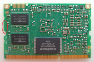
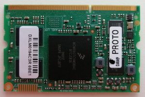
- PCB version is copper printed on PCB itself, as shown in Fig. 1
- serial number: it is printed on a white label, as shown in Fig. 2: see also Product serial number page for more details
- ConfigID: it is used by software running on the board for the identification of the product model/hardware configuration. For more details, please refer to this link
- On AXEL Lite SOM ConfigID is stored in these areas of OTP
Part number composition[edit | edit source]
AXEL Lite SOM module part number is identified by the following digit-code table:
| Part number structure | Options | Description |
|---|---|---|
| Family | DXL | Family prefix code |
| SOC |
|
System On Chip definition |
| NOR SPI |
|
Flash memory NOR size |
| RAM |
|
DDR memory RAM size |
| NAND |
|
Flash memory NAND size |
| Boot/bus width |
|
Boot options and RAM Bus width |
| Temperature range |
|
For the DAVE Embedded Systems' product Temperature Range classification, please find more information at the page Products Classification |
| PCB revision |
|
PCB release may change for manufacturing purposes (i.e. text fixture adaptation) |
| Manufacturing option | R: RoHS | typically connected to production process and quality |
| Software Configuration |
|
If customers require custom SW deployed this section should be defined and agreed |
Example[edit | edit source]
AXEL Lite SOM code DXLM0213C3R-00
- DXL - AXEL Lite SOM module
- M - i.MX6 DualLite 800MHz -40/105°C
- 0 - NO NOR SPI onboard
- 2 - 2GB DDR3
- 1 - 1GB NAND SLC
- 3 - boot from NAND/SD wuth 64 bit bus width
- C - Commercial tamperature range (i.e. 0/95°C)
- 3 - PCB revision C
- R - RoHS manufacturing process
- -00 standard factory u-boot pre-programmed
Pinout Table[edit | edit source]
Connectors and Pinout Table[edit | edit source]
Connectors description[edit | edit source]
In the following table are described all available connectors integrated on AXEL Lite SOM:
| Connector name | Connector Type | Notes | Carrier board counterpart |
|---|---|---|---|
| J1 | SODIMM DDR3 edge connector 204 pin | TE Connectivity 2-2013289-1 |
The dedicated carrier board must mount the mating connector and connect the desired peripheral interfaces according to AXEL Lite pinout specifications. See the images below for reference:
Pinout table naming conventions[edit | edit source]
This chapter contains the pinout description of the AXEL Lite SOM module, grouped in two tables (odd and even pins) that report the pin mapping of the 204-pin SO-DIMM connector.
Each row in the pinout tables contains the following information:
| Pin | Reference to the connector pin |
| Pin Name | Pin (signal) name on the AxelLite connectors |
| Internal connections |
Connections to the components
|
| Ball/pin # | Component ball/pin number connected to signal |
| Voltage domain | The voltage domain the pin belongs to |
| Type | Pin type:
|
| Notes | Remarks on special pin characteristics |
| Pin MUX alternative functions | Muxes:
|
Voltage domains[edit | edit source]
| Voltage domain | Nominal voltage [V] | Notes |
|---|---|---|
| 3.3VIN | 3.3 | See Operational_characteristics of the SoM wiki page |
| VCC_ENET_1V8 | 1.8 | Voltage generated by the internal PSU. See Power Supply Unit (PSU) wiki page |
| AXEL_IO_3V3 | 3.3 | Voltage generated by the internal PSU. See Power Supply Unit (PSU) wiki page |
| GEN_2V5 | 2.5 | Voltage generated by the internal PSU. See Power Supply Unit (PSU) wiki page |
SODIMM ODD pins declaration[edit | edit source]
| Pin | Pin Name | Internal Connections | Ball/pin # | Voltage
domain |
Type | Notes | Alternative Functions | |
|---|---|---|---|---|---|---|---|---|
| J2.1 | DGND | DGND | - | - | G | |||
| J2.3 | 3.3VIN | INPUT VOLTAGE | - | 3.3VIN | S | |||
| J2.5 | 3.3VIN | INPUT VOLTAGE | - | 3.3VIN | S | |||
| J2.7 | 3.3VIN | INPUT VOLTAGE | - | 3.3VIN | S | |||
| J2.9 | 3.3VIN | INPUT VOLTAGE | - | 3.3VIN | S | |||
| J2.11 | DGND | DGND | - | - | G | |||
| J2.13 | ETH0_LED1 | LAN.LED1/PME_N1 | 17 | VCC_ENET_1V8 | O | Internal 10k pull-up to 1.8V
This signal requires voltage level shifters if used at 3.3V |
||
| J2.15 | ETH0_LED2 | LAN.LED2 | 15 | VCC_ENET_1V8 | O | Internal 10k pull-up to 1.8V
This signal requires voltage level shifters if used at 3.3V |
||
| J2.17 | DGND | DGND | - | - | G | |||
| J2.19 | ETH0_TXRX0_P | LAN.TXRXP_A | 2 | AXEL_IO_3V3 | D | |||
| J2.21 | ETH0_TXRX0_M | LAN.TXRXM_A | 3 | AXEL_IO_3V3 | D | |||
| J2.23 | ETH0_TXRX1_P | LAN.TXRXP_B | 5 | AXEL_IO_3V3 | D | |||
| J2.25 | ETH0_TXRX1_M | LAN.TXRXM_B | 6 | AXEL_IO_3V3 | D | |||
| J2.27 | ETH0_TXRX2_P | LAN.TXRXP_C | 7 | AXEL_IO_3V3 | D | |||
| J2.29 | ETH0_TXRX2_M | LAN.TXRXM_C | 8 | AXEL_IO_3V3 | D | |||
| J2.31 | ETH0_TXRX3_P | LAN.TXRXP_D | 10 | AXEL_IO_3V3 | D | |||
| J2.33 | ETH0_TXRX3_M | LAN.TXRXM_D | 11 | AXEL_IO_3V3 | D | |||
| J2.35 | DGND | DGND | - | - | G | |||
| J2.37 | SD3_RST | CPU.SD3_RST | D15 | AXEL_IO_3V3 | IO | Pin ALT-0 | SD3_RESET | |
| Pin ALT-1 | UART3_RTS_B | |||||||
| Pin ALT-5 | GPIO7_IO08 | |||||||
| J2.39 | SD3_DATA0 | CPU.SD3_DATA0 | E14 | AXEL_IO_3V3 | IO | Pin ALT-0 | SD3_DATA0 | |
| Pin ALT-1 | UART1_CTS_B | |||||||
| Pin ALT-2 | FLEXCAN2_TX | |||||||
| Pin ALT-5 | GPIO7_IO04 | |||||||
| J2.41 | SD3_DATA1 | CPU.SD3_DATA1 | F14 | AXEL_IO_3V3 | IO | Pin ALT-0 | SD3_DATA1 | |
| Pin ALT-1 | UART1_RTS_B | |||||||
| Pin ALT-2 | FLEXCAN2_RX | |||||||
| Pin ALT-5 | GPIO7_IO05 | |||||||
| J2.43 | SD3_DATA2 | CPU.SD3_DATA2 | A15 | AXEL_IO_3V3 | IO | Pin ALT-0 | SD3_DATA2 | |
| Pin ALT-5 | GPIO7_IO06 | |||||||
| J2.45 | SD3_DATA3 | CPU.SD3_DATA3 | B15 | AXEL_IO_3V3 | IO | Pin ALT-0 | SD3_DATA3 | |
| Pin ALT-1 | UART3_CTS_B | |||||||
| Pin ALT-5 | GPIO7_IO07 | |||||||
| J2.47 | SD3_DATA4 | CPU.SD3_DATA4 | D13 | AXEL_IO_3V3 | IO | Pin ALT-0 | SD3_DATA4 | |
| Pin ALT-1 | UART2_RX_DATA | |||||||
| Pin ALT-5 | GPIO7_IO01 | |||||||
| J2.49 | SD3_DATA5 | CPU.SD3_DATA5 | C13 | AXEL_IO_3V3 | IO | Pin ALT-0 | SD3_DATA5 | |
| Pin ALT-1 | UART2_TX_DATA | |||||||
| Pin ALT-5 | GPIO7_IO00 | |||||||
| J2.51 | SD3_DATA6 | CPU.SD3_DATA6 | E13 | AXEL_IO_3V3 | IO | Pin ALT-0 | SD3_DATA6 | |
| Pin ALT-1 | UART1_RX_DATA | |||||||
| Pin ALT-5 | GPIO6_IO18 | |||||||
| J2.53 | SD3_DATA7 | CPU.SD3_DATA7 | F13 | AXEL_IO_3V3 | IO | Pin ALT-0 | SD3_DATA7 | |
| Pin ALT-1 | UART1_TX_DATA | |||||||
| Pin ALT-5 | GPIO6_IO17 | |||||||
| J2.55 | SD3_CMD | CPU.SD3_CMD | B13 | AXEL_IO_3V3 | IO | Pin ALT-0 | SD3_CMD | |
| Pin ALT-1 | UART2_CTS_B | |||||||
| Pin ALT-2 | FLEXCAN1_TX | |||||||
| Pin ALT-5 | GPIO7_IO02 | |||||||
| J2.57 | DGND | DGND | - | - | G | |||
| J2.59 | SD3_CLK | CPU.SD3_CLK | D14 | AXEL_IO_3V3 | IO | Pin ALT-0 | SD3_CLK | |
| Pin ALT-1 | UART2_RTS_B | |||||||
| Pin ALT-2 | UART2_RTS_B | |||||||
| Pin ALT-5 | GPIO7_IO03 | |||||||
| J2.61 | SD2_DATA0 | CPU.SD2_DATA0 | A22 | AXEL_IO_3V3 | IO | Pin ALT-0 | SD2_DATA0 | |
| Pin ALT-1 | ECSPI5_MISO | |||||||
| Pin ALT-3 | AUD4_RXD | |||||||
| Pin ALT-4 | KEY_ROW7 | |||||||
| Pin ALT-5 | GPIO1_IO15 | |||||||
| Pin ALT-6 | DCIC2_OUT | |||||||
| J2.63 | SD2_DATA1 | CPU.SD2_DATA1 | E20 | AXEL_IO_3V3 | IO | Pin ALT-0 | SD2_DATA1 | |
| Pin ALT-1 | ECSPI5_SS0 | |||||||
| Pin ALT-2 | EIM_CS2 | |||||||
| Pin ALT-3 | AUD4_TXFS | |||||||
| Pin ALT-4 | KEY_COL7 | |||||||
| Pin ALT-5 | GPIO1_IO14 | |||||||
| J2.65 | SD2_DATA2 | CPU.SD2_DATA2 | A23 | AXEL_IO_3V3 | IO | Pin ALT-0 | SD2_DATA2 | |
| Pin ALT-1 | ECSPI5_SS1 | |||||||
| Pin ALT-2 | EIM_CS3 | |||||||
| Pin ALT-3 | AUD4_TXD | |||||||
| Pin ALT-4 | KEY_ROW6 | |||||||
| Pin ALT-5 | GPIO1_IO13 | |||||||
| J2.67 | SD2_DATA3 | CPU.SD2_DATA3 | B22 | AXEL_IO_3V3 | IO | Pin ALT-0 | SD2_DATA3 | |
| Pin ALT-1 | ECSPI5_SS3 | |||||||
| Pin ALT-2 | ECSPI5_SS3 | |||||||
| Pin ALT-3 | AUD4_TXC | |||||||
| Pin ALT-5 | GPIO1_IO12 | |||||||
| J2.69 | SD2_CMD | CPU.SD2_CMD | F19 | AXEL_IO_3V3 | IO | Pin ALT-0 | SD2_CMD | |
| Pin ALT-1 | ECSPI5_MOSI | |||||||
| Pin ALT-2 | KEY_ROW5 | |||||||
| Pin ALT-3 | AUD4_RXC | |||||||
| Pin ALT-5 | GPIO1_IO11 | |||||||
| J2.71 | SD2_CLK | CPU.SD2_CLK | C21 | AXEL_IO_3V3 | IO | Pin ALT-0 | SD2_CLK | |
| Pin ALT-1 | ECSPI5_SCLK | |||||||
| Pin ALT-2 | KEY_COL5 | |||||||
| Pin ALT-3 | AUD4_RXFS | |||||||
| Pin ALT-5 | GPIO1_IO10 | |||||||
| J2.73 | DGND | DGND | - | - | G | |||
| J2.75 | SD1_DAT0 | CPU.SD1_DAT0 | A21 | AXEL_IO_3V3 | IO | Pin ALT-0 | SD1_DATA0 | |
| Pin ALT-1 | ECSPI5_MISO | |||||||
| Pin ALT-2 | GPT_CAPTURE1 | |||||||
| Pin ALT-5 | GPIO1_IO16 | |||||||
| J2.77 | SD1_DAT1 | CPU.SD1_DAT1 | C20 | AXEL_IO_3V3 | IO | Pin ALT-0 | SD1_DATA1 | |
| Pin ALT-1 | ECSPI5_SS0 | |||||||
| Pin ALT-2 | PWM3_OUT | |||||||
| Pin ALT-3 | GPT_CAPTURE2 | |||||||
| Pin ALT-5 | GPIO1_IO17 | |||||||
| J2.79 | SD1_DAT2 | CPU.SD1_DAT2 | E19 | AXEL_IO_3V3 | IO | Pin ALT-0 | SD1_DATA2 | |
| Pin ALT-1 | ECSPI5_SS1 | |||||||
| Pin ALT-2 | GPT_COMPARE2 | |||||||
| Pin ALT-3 | PWM2_OUT | |||||||
| Pin ALT-4 | WDOG1_B | |||||||
| Pin ALT-5 | GPIO1_IO19 | |||||||
| Pin ALT-6 | WDOG1_RESET_B_DEB | |||||||
| J2.81 | SD1_DAT3 | CPU.SD1_DAT3 | F18 | AXEL_IO_3V3 | IO | Pin ALT-0 | SD1_DATA3 | |
| Pin ALT-1 | ECSPI5_SS2 | |||||||
| Pin ALT-2 | GPT_COMPARE3 | |||||||
| Pin ALT-3 | PWM1_OUT | |||||||
| Pin ALT-4 | WDOG2_B | |||||||
| Pin ALT-5 | GPIO1_IO21 | |||||||
| Pin ALT-6 | WDOG2_RESET_B_DEB | |||||||
| J2.83 | SD1_CMD | CPU.SD1_CMD | B21 | AXEL_IO_3V3 | IO | Pin ALT-0 | SD1_CMD | |
| Pin ALT-1 | ECSPI5_MOSI | |||||||
| Pin ALT-2 | PWM4_OUT | |||||||
| Pin ALT-3 | GPT_COMPARE1 | |||||||
| Pin ALT-5 | GPIO1_IO18 | |||||||
| J2.85 | SD1_CLK | CPU.SD1_CLK | D20 | AXEL_IO_3V3 | IO | Pin ALT-0 | SD1_CLK | |
| Pin ALT-1 | ECSPI5_SCLK | |||||||
| Pin ALT-3 | GPT_CLKIN | |||||||
| Pin ALT-5 | GPIO1_IO20 | |||||||
| J2.87 | DGND | DGND | - | - | G | |||
| J2.89 | KEY_COL0/|ECSPI1_SCLK | CPU.KEY_COL0 | W5 | AXEL_IO_3V3 | IO | Pin ALT-0 | ECSPI1_SCLK | |
| Pin ALT-1 | ENET_RX_DATA3 | |||||||
| Pin ALT-2 | AUD5_TXC | |||||||
| Pin ALT-3 | KEY_COL0 | |||||||
| Pin ALT-4 | UART4_TX_DATA | |||||||
| Pin ALT-5 | GPIO4_IO06 | |||||||
| Pin ALT-6 | DCIC1_OUT | |||||||
| J2.91 | KEY_ROW0/|ECSPI1_MOSI | CPU.KEY_ROW0 | V6 | AXEL_IO_3V3 | IO | Pin ALT-0 | ECSPI1_MOSI | |
| Pin ALT-1 | ENET_TX_DATA3 | |||||||
| Pin ALT-2 | AUD5_TXD | |||||||
| Pin ALT-3 | KEY_ROW0 | |||||||
| Pin ALT-4 | UART4_RX_DATA | |||||||
| Pin ALT-5 | GPIO4_IO07 | |||||||
| Pin ALT-6 | DCIC2_OUT | |||||||
| J2.93 | KEY_COL1/|ECSPI1_MISO | CPU.KEY_COL1 | U7 | AXEL_IO_3V3 | IO | Pin ALT-0 | ECSPI1_MISO | |
| Pin ALT-1 | ENET_MDIO | |||||||
| Pin ALT-2 | AUD5_TXFS | |||||||
| Pin ALT-3 | KEY_COL1 | |||||||
| Pin ALT-4 | UART5_TX_DATA | |||||||
| Pin ALT-5 | GPIO4_IO08 | |||||||
| Pin ALT-6 | SD1_VSELECT | |||||||
| J2.95 | KEY_ROW1/|ECSPI1_SS0 | CPU.KEY_ROW1 | U6 | AXEL_IO_3V3 | IO | Pin ALT-0 | ECSPI1_SS0 | |
| Pin ALT-1 | ENET_COL | |||||||
| Pin ALT-2 | AUD5_RXD | |||||||
| Pin ALT-3 | KEY_ROW1 | |||||||
| Pin ALT-4 | UART5_RX_DATA | |||||||
| Pin ALT-5 | GPIO4_IO09 | |||||||
| Pin ALT-6 | SD2_VSELECT | |||||||
| J2.97 | KEY_COL2/|ECSPI1_SS1 | CPU.KEY_COL2 | W6 | AXEL_IO_3V3 | IO | Pin ALT-0 | ECSPI1_SS1 | |
| Pin ALT-1 | ENET_RX_DATA2 | |||||||
| Pin ALT-2 | FLEXCAN1_TX | |||||||
| Pin ALT-3 | KEY_COL2 | |||||||
| Pin ALT-4 | ENET_MDC | |||||||
| Pin ALT-5 | GPIO4_IO10 | |||||||
| Pin ALT-6 | USB_H1_PWR_CTL_WAKE | |||||||
| J2.99 | KEY_ROW2 | CPU.KEY_ROW2 | W4 | AXEL_IO_3V3 | IO | Pin ALT-0 | ECSPI1_SS2 | |
| Pin ALT-1 | ENET_TX_DATA2 | |||||||
| Pin ALT-2 | FLEXCAN1_RX | |||||||
| Pin ALT-3 | KEY_ROW2 | |||||||
| Pin ALT-4 | SD2_VSELECT | |||||||
| Pin ALT-5 | GPIO4_IO11 | |||||||
| Pin ALT-6 | HDMI_TX_CEC_LINE | |||||||
| J2.101 | KEY_COL3/|I2C2_SCL | CPU.KEY_COL3 | U5 | AXEL_IO_3V3 | IO | Internally connected to PMIC I2C interface | Pin ALT-0 | ECSPI1_SS3 |
| Pin ALT-1 | ENET_CRS | |||||||
| Pin ALT-3 | HDMI_TX_DDC_SCL | |||||||
| Pin ALT-4 | KEY_COL3 | |||||||
| Pin ALT-4 | I2C2_SCL | |||||||
| Pin ALT-5 | GPIO4_IO12 | |||||||
| Pin ALT-6 | SPDIF_IN | |||||||
| J2.103 | KEY_ROW3/|I2C2_SDA | CPU.KEY_ROW3 | T7 | AXEL_IO_3V3 | IO | Internally connected to PMIC I2C interface | Pin ALT-1 | ASRC_EXT_CLK |
| Pin ALT-2 | HDMI_TX_DDC_SDA | |||||||
| Pin ALT-3 | KEY_ROW3 | |||||||
| Pin ALT-4 | I2C2_SDA | |||||||
| Pin ALT-5 | GPIO4_IO13 | |||||||
| Pin ALT-6 | SD1_VSELECT | |||||||
| J2.105 | KEY_COL4 | CPU.KEY_COL4 | T6 | AXEL_IO_3V3 | IO | Pin ALT-0 | FLEXCAN2_TX | |
| Pin ALT-1 | IPU1_SISG4 | |||||||
| Pin ALT-2 | USB_OTG_OC | |||||||
| Pin ALT-3 | KEY_COL4 | |||||||
| Pin ALT-4 | UART5_RTS_B | |||||||
| Pin ALT-5 | GPIO4_IO14 | |||||||
| J2.107 | KEY_ROW4 | CPU.KEY_ROW4 | V5 | AXEL_IO_3V3 | IO | Pin ALT-0 | FLEXCAN2_RX | |
| Pin ALT-1 | IPU1_SISG5 | |||||||
| Pin ALT-2 | USB_OTG_PWR | |||||||
| Pin ALT-3 | KEY_ROW4 | |||||||
| Pin ALT-4 | UART5_CTS_B | |||||||
| Pin ALT-5 | GPIO4_IO15 | |||||||
| J2.109 | DGND | DGND | - | - | G | |||
| J2.111 | HDMI_CLKN | CPU.HDMI_CLKN | J5 | GEN_2V5 | D | |||
| J2.113 | HDMI_CLKP | CPU.HDMI_CLKP | J6 | GEN_2V5 | D | |||
| J2.115 | HDMI_D0N | CPU.HDMI_D0N | K5 | GEN_2V5 | D | |||
| J2.117 | HDMI_D0P | CPU.HDMI_D0P | K6 | GEN_2V5 | D | |||
| J2.119 | HDMI_D1N | CPU.HDMI_D1N | J3 | GEN_2V5 | D | |||
| J2.121 | HDMI_D1P | CPU.HDMI_D1P | J4 | GEN_2V5 | D | |||
| J2.123 | HDMI_D2N | CPU.HDMI_D2N | K3 | GEN_2V5 | D | |||
| J2.125 | HDMI_D2P | CPU.HDMI_D2P | K4 | GEN_2V5 | D | |||
| J2.127 | HDMI_CEC_IN | CPU.HDMI_DDCCEC | K2 | GEN_2V5 | D | |||
| J2.129 | HDMI_HPD | CPU.HDMI_HPD | K1 | GEN_2V5 | D | |||
| J2.131 | DGND | DGND | - | - | G | |||
| J2.133 | LVDS0_CLK_N | CPU.LVDS0_CLK_N | V4 | GEN_2V5 | D | |||
| J2.135 | LVDS0_CLK_P | CPU.LVDS0_CLK_P | V3 | GEN_2V5 | D | |||
| J2.137 | LVDS0_TX0_N | CPU.LVDS0_TX0_N | U2 | GEN_2V5 | D | |||
| J2.139 | LVDS0_TX0_P | CPU.LVDS0_TX0_P | U1 | GEN_2V5 | D | |||
| J2.141 | LVDS0_TX1_N | CPU.LVDS0_TX1_N | U4 | GEN_2V5 | D | |||
| J2.143 | LVDS0_TX1_P | CPU.LVDS0_TX1_P | U3 | GEN_2V5 | D | |||
| J2.145 | LVDS0_TX2_N | CPU.LVDS0_TX2_N | V2 | GEN_2V5 | D | |||
| J2.147 | LVDS0_TX2_P | CPU.LVDS0_TX2_P | V1 | GEN_2V5 | D | |||
| J2.149 | LVDS0_TX3_N | CPU.LVDS0_TX3_N | W2 | GEN_2V5 | D | |||
| J2.151 | LVDS0_TX3_P | CPU.LVDS0_TX3_P | W1 | GEN_2V5 | D | |||
| J2.153 | DGND | DGND | - | - | G | |||
| J2.155 | LVDS1_CLK_N | CPU.LVDS1_CLK_N | Y3 | GEN_2V5 | D | |||
| J2.157 | LVDS1_CLK_P | CPU.LVDS1_CLK_P | Y4 | GEN_2V5 | D | |||
| J2.159 | LVDS1_TX0_N | CPU.LVDS1_TX0_N | Y1 | GEN_2V5 | D | |||
| J2.161 | LVDS1_TX0_P | CPU.LVDS1_TX0_P | Y2 | GEN_2V5 | D | |||
| J2.163 | LVDS1_TX1_N | CPU.LVDS1_TX1_N | AA2 | GEN_2V5 | D | |||
| J2.165 | LVDS1_TX1_P | CPU.LVDS1_TX1_P | AA1 | GEN_2V5 | D | |||
| J2.167 | LVDS1_TX2_N | CPU.LVDS1_TX2_N | AB1 | GEN_2V5 | D | |||
| J2.169 | LVDS1_TX2_P | CPU.LVDS1_TX2_P | AB2 | GEN_2V5 | D | |||
| J2.171 | LVDS1_TX3_N | CPU.LVDS1_TX3_N | AA3 | GEN_2V5 | D | |||
| J2.173 | LVDS1_TX3_P | CPU.LVDS1_TX3_P | AA4 | GEN_2V5 | D | |||
| J2.175 | DGND | DGND | - | - | G | |||
| J2.177 | EIM_D19 | CPU.EIM_D19 | G21 | AXEL_IO_3V3 | IO | Pin ALT-0 | ECSPI1_SS1 | |
| Pin ALT-1 | IPU1_DI0_PIN08 | |||||||
| Pin ALT-2 | IPU2_CSI1_DATA16 | |||||||
| Pin ALT-3 | UART1_CTS_B | |||||||
| Pin ALT-4 | GPIO3_IO19 | |||||||
| Pin ALT-5 | EPIT1_OUT | |||||||
| Pin ALT-7 | EPDC_DATA12 | |||||||
| J2.179 | EIM_D20 | CPU.EIM_D20 | G20 | AXEL_IO_3V3 | IO | Pin ALT-0 | ECSPI4_SS0 | |
| Pin ALT-1 | IPU1_DI0_PIN16 | |||||||
| Pin ALT-2 | IPU2_CSI1_DATA15 | |||||||
| Pin ALT-3 | UART1_RTS_B | |||||||
| Pin ALT-4 | GPIO3_IO20 | |||||||
| Pin ALT-5 | EPIT2_OUT | |||||||
| J2.181 | EIM_D21 | CPU.EIM_D21 | H20 | AXEL_IO_3V3 | IO | Pin ALT-0 | ECSPI4_SCLK | |
| Pin ALT-1 | IPU1_DI0_PIN17 | |||||||
| Pin ALT-2 | IPU2_CSI1_DATA11 | |||||||
| Pin ALT-3 | USB_OTG_OC | |||||||
| Pin ALT-4 | GPIO3_IO21 | |||||||
| Pin ALT-5 | I2C1_SCL | |||||||
| Pin ALT-6 | SPDIF_IN | |||||||
| J2.183 | EIM_D22 | CPU.EIM_D22 | E23 | AXEL_IO_3V3 | IO | Pin ALT-0 | ECSPI4_MISO | |
| Pin ALT-1 | IPU1_DI0_PIN01 | |||||||
| Pin ALT-2 | IPU2_CSI1_DATA10 | |||||||
| Pin ALT-3 | USB_OTG_PWR | |||||||
| Pin ALT-4 | GPIO3_IO22 | |||||||
| Pin ALT-5 | SPDIF_OUT | |||||||
| Pin ALT-7 | EPDC_SDCE6 | |||||||
| J2.185 | EIM_D23 | CPU.EIM_D23 | D25 | AXEL_IO_3V3 | IO | Pin ALT-0 | IPU1_DI0_D0_CS | |
| Pin ALT-1 | UART3_CTS_B | |||||||
| Pin ALT-2 | UART1_DCD_B | |||||||
| Pin ALT-3 | IPU2_CSI1_DATA_EN | |||||||
| Pin ALT-4 | GPIO3_IO23 | |||||||
| Pin ALT-5 | IPU1_DI1_PIN02 | |||||||
| Pin ALT-6 | IPU1_DI1_PIN14 | |||||||
| Pin ALT-7 | EPDC_DATA11 | |||||||
| J2.187 | EIM_D24 | CPU.EIM_D24 | F22 | AXEL_IO_3V3 | IO | Pin ALT-0 | ECSPI4_SS2 | |
| Pin ALT-1 | UART3_TX_DATA | |||||||
| Pin ALT-2 | ECSPI1_SS2 | |||||||
| Pin ALT-3 | ECSPI2_SS2 | |||||||
| Pin ALT-4 | GPIO3_IO24 | |||||||
| Pin ALT-5 | AUD5_RXFS | |||||||
| Pin ALT-6 | UART1_DTR_B | |||||||
| Pin ALT-7 | EPDC_SDCE7 | |||||||
| J2.189 | EIM_D25 | CPU.EIM_D25 | G22 | AXEL_IO_3V3 | IO | Pin ALT-0 | ECSPI4_SS3 | |
| Pin ALT-1 | UART3_RX_DATA | |||||||
| Pin ALT-2 | ECSPI1_SS3 | |||||||
| Pin ALT-3 | ECSPI2_SS3 | |||||||
| Pin ALT-4 | GPIO3_IO25 | |||||||
| Pin ALT-5 | AUD5_RXC | |||||||
| Pin ALT-6 | UART1_DSR_B | |||||||
| Pin ALT-7 | EPDC_SDCE8 | |||||||
| J2.191 | EIM_D26 | CPU.EIM_D26 | E24 | AXEL_IO_3V3 | IO | Pin ALT-0 | IPU1_DI1_PIN11 | |
| Pin ALT-1 | IPU1_CSI0_DATA01 | |||||||
| Pin ALT-2 | IPU2_CSI1_DATA14 | |||||||
| Pin ALT-3 | UART2_TX_DATA | |||||||
| Pin ALT-4 | GPIO3_IO26 | |||||||
| Pin ALT-5 | IPU1_SISG2 | |||||||
| Pin ALT-6 | IPU1_DISP1_DATA22 | |||||||
| Pin ALT-7 | EPDC_SDOED | |||||||
| J2.193 | EIM_D27 | CPU.EIM_D27 | E25 | AXEL_IO_3V3 | IO | Pin ALT-0 | IPU1_DI1_PIN13 | |
| Pin ALT-1 | IPU1_CSI0_DATA00 | |||||||
| Pin ALT-2 | IPU2_CSI1_DATA13 | |||||||
| Pin ALT-3 | UART2_RX_DATA | |||||||
| Pin ALT-4 | GPIO3_IO27 | |||||||
| Pin ALT-5 | IPU1_SISG3 | |||||||
| Pin ALT-6 | IPU1_DISP1_DATA23 | |||||||
| Pin ALT-7 | EPDC_SDOE | |||||||
| J2.195 | EIM_D28 | CPU.EIM_D28 | G23 | AXEL_IO_3V3 | IO | Pin ALT-0 | I2C1_SDA | |
| Pin ALT-1 | ECSPI4_MOSI | |||||||
| Pin ALT-2 | IPU2_CSI1_DATA12 | |||||||
| Pin ALT-3 | UART2_CTS_B | |||||||
| Pin ALT-4 | GPIO3_IO28 | |||||||
| Pin ALT-5 | IPU1_EXT_TRIG | |||||||
| Pin ALT-6 | IPU1_DI0_PIN13 | |||||||
| Pin ALT-7 | EPDC_PWR_CTRL3 | |||||||
| J2.197 | EIM_D29 | CPU.EIM_D29 | J19 | AXEL_IO_3V3 | IO | Pin ALT-0 | IPU1_DI1_PIN15 | |
| Pin ALT-1 | ECSPI4_SS0 | |||||||
| Pin ALT-3 | UART2_RTS_B | |||||||
| Pin ALT-4 | GPIO3_IO29 | |||||||
| Pin ALT-5 | IPU2_CSI1_VSYNC | |||||||
| Pin ALT-6 | IPU1_DI0_PIN14 | |||||||
| Pin ALT-7 | EPDC_PWR_WAKE | |||||||
| J2.199 | EIM_D30 | CPU.EIM_D30 | J20 | AXEL_IO_3V3 | IO | Pin ALT-0 | IPU1_DISP1_DATA21 | |
| Pin ALT-1 | IPU1_DI0_PIN11 | |||||||
| Pin ALT-2 | IPU1_CSI0_DATA03 | |||||||
| Pin ALT-3 | UART3_CTS_B | |||||||
| Pin ALT-4 | GPIO3_IO30 | |||||||
| Pin ALT-5 | USB_H1_OC | |||||||
| Pin ALT-7 | EPDC_SDOEZ | |||||||
| J2.201 | EIM_D31 | CPU.EIM_D31 | H21 | AXEL_IO_3V3 | IO | Pin ALT-0 | IPU1_DISP1_DATA20 | |
| Pin ALT-1 | IPU1_DI0_PIN12 | |||||||
| Pin ALT-2 | IPU1_CSI0_DATA02 | |||||||
| Pin ALT-3 | UART3_RTS_B | |||||||
| Pin ALT-4 | GPIO3_IO31 | |||||||
| Pin ALT-5 | USB_H1_PWR | |||||||
| Pin ALT-7 | EPDC_SDCLK_P | |||||||
| Pin ALT-8 | EIM_ACLK_FREERUN | |||||||
| J2.203 | DGND | DGND | - | - | G | |||
SODIMM EVEN pins declaration[edit | edit source]
| Pin | Pin Name | Internal Connections | Ball/pin # | Voltage|domain | Type | Notes | Alternative Functions | |
|---|---|---|---|---|---|---|---|---|
| J2.2 | DGND | DGND | - | - | G | |||
| J2.4 | 3.3VIN | INPUT VOLTAGE | - | 3.3VIN | S | |||
| J2.6 | 3.3VIN | INPUT VOLTAGE | - | 3.3VIN | S | |||
| J2.8 | 3.3VIN | INPUT VOLTAGE | - | 3.3VIN | S | |||
| J2.10 | 3.3VIN | INPUT VOLTAGE | - | 3.3VIN | S | |||
| J2.12 | DGND | DGND | - | - | G | |||
| J2.14 | PMIC_LICELL | PMIC.LICELL | 42 |
|
||||
| J2.16 | CPU_ONOFF | CPU.CPU_ONOFF | D12 | |||||
| J2.18 | BOARD_PGOOD | - | - | |||||
| J2.20 | BOOT_MODE_SEL | BOOT MODE SELECTION | This is a pulled-up input. Leave unconnected to select "1". Connect to ground to select "0". For more details, please see also the following pages: | |||||
| J2.22 | CPU_PORn | CPU.CPU_PORn | C11 | |||||
| J2.24 | PMIC_PWRON | PMIC.PWRON | 56 | |||||
| J2.26 | GPIO_0 | CPU.GPIO_0 | T5 | AXEL_IO_3V3 | IO | Pin ALT-0 | CCM_CLKO1 | |
| Pin ALT-2 | KEY_COL5 | |||||||
| Pin ALT-3 | ASRC_EXT_CLK | |||||||
| Pin ALT-5 | GPIO1_IO00 | |||||||
| Pin ALT-6 | USB_H1_PWR | |||||||
| Pin ALT-7 | SNVS_VIO_5 | |||||||
| J2.28 | GPIO_1 | CPU.GPIO_1 | T4 | AXEL_IO_3V3 | IO | Reset_scheme_and_control_signals#Handling_CPU-initiated_software_reset | Pin ALT-0 | ESAI_RX_CLK |
| Pin ALT-1 | WDOG2_B | |||||||
| Pin ALT-2 | KEY_ROW5 | |||||||
| Pin ALT-3 | USB_OTG_ID | |||||||
| Pin ALT-4 | PWM2_OUT | |||||||
| Pin ALT-5 | GPIO1_IO01 | |||||||
| Pin ALT-6 | SD1_CD_B | |||||||
| J2.30 | DGND | DGND | - | - | G | |||
| J2.32 | GPIO_2 | CPU.GPIO_2 | T1 | AXEL_IO_3V3 | IO | Pin ALT-0 | ESAI_TX_FS | |
| Pin ALT-2 | KEY_ROW6 | |||||||
| Pin ALT-5 | GPIO1_IO02 | |||||||
| Pin ALT-6 | SD2_WP | |||||||
| Pin ALT-7 | MLB_DATA | |||||||
| J2.34 | GPIO_3/I2C3_SCL | CPU.GPIO_3 | R7 | AXEL_IO_3V3 | IO | Pin ALT-0 | ESAI_RX_HF_CLK | |
| Pin ALT-2 | I2C3_SCL | |||||||
| Pin ALT-3 | XTALOSC_REF_CLK_24M | |||||||
| Pin ALT-4 | CCM_CLKO2 | |||||||
| Pin ALT-5 | GPIO1_IO03 | |||||||
| Pin ALT-6 | USB_H1_OC | |||||||
| Pin ALT-7 | MLB_CLK | |||||||
| J2.36 | GPIO_4 | CPU.GPIO_4 | R6 | AXEL_IO_3V3 | IO | Pin ALT-0 | ESAI_TX_HF_CLK | |
| Pin ALT-2 | KEY_COL7 | |||||||
| Pin ALT-5 | GPIO1_IO04 | |||||||
| Pin ALT-6 | SD2_CD_B | |||||||
| J2.38 | GPIO_5 | CPU.GPIO_5 | R4 | AXEL_IO_3V3 | IO | Pin ALT-0 | ESAI_TX2_RX3 | |
| Pin ALT-2 | KEY_ROW7 | |||||||
| Pin ALT-3 | CCM_CLKO1 | |||||||
| Pin ALT-5 | GPIO1_IO05 | |||||||
| Pin ALT-6 | I2C3_SCL | |||||||
| Pin ALT-7 | ARM_EVENTI | |||||||
| J2.40 | GPIO_6/I2C3_SDA | CPU.GPIO_6 | T3 | AXEL_IO_3V3 | IO | Pin ALT-0 | ESAI_TX_CLK | |
| Pin ALT-2 | I2C3_SDA | |||||||
| Pin ALT-5 | GPIO1_IO06 | |||||||
| Pin ALT-6 | SD2_LCTL | |||||||
| Pin ALT-7 | MLB_SIG | |||||||
| J2.42 | GPIO_7//FLEXCAN1_H | CPU.GPIO_7 | R3 | AXEL_IO_3V3 | IO | Hardware mounting option depending on order code|CAN_TX (PHY onboard) or GPIO_7 | Pin ALT-0 | ESAI_TX4_RX1 |
| Pin ALT-1 | ECSPI5_RDY | |||||||
| Pin ALT-2 | EPIT1_OUT | |||||||
| Pin ALT-3 | FLEXCAN1_TX | |||||||
| Pin ALT-4 | UART2_TX_DATA | |||||||
| Pin ALT-5 | GPIO1_IO07 | |||||||
| Pin ALT-6 | SPDIF_LOCK | |||||||
| Pin ALT-7 | USB_OTG_HOST_MODE | |||||||
| Pin ALT-8 | I2C4_SCL | |||||||
| J2.44 | GPIO_8//FLEXCAN1_L | CPU.GPIO_8 | R5 | AXEL_IO_3V3 | IO | Hardware mounting option depending on order code|CAN_RX (PHY onboard) or GPIO_8 | Pin ALT-0 | ESAI_TX5_RX0 |
| Pin ALT-1 | XTALOSC_REF_CLK_32K | |||||||
| Pin ALT-2 | EPIT2_OUT | |||||||
| Pin ALT-3 | FLEXCAN1_RX | |||||||
| Pin ALT-4 | UART2_RX_DATA | |||||||
| Pin ALT-5 | GPIO1_IO08 | |||||||
| Pin ALT-6 | SPDIF_SR_CLK | |||||||
| Pin ALT-7 | USB_OTG_PWR_CTL_WAKE | |||||||
| Pin ALT-8 | I2C4_SDA | |||||||
| J2.46 | GPIO_9 | CPU.GPIO_9 | T2 | AXEL_IO_3V3 | IO | Pin ALT-0 | ESAI_RX_FS | |
| Pin ALT-1 | WDOG1_B | |||||||
| Pin ALT-2 | KEY_COL6 | |||||||
| Pin ALT-3 | CCM_REF_EN_B | |||||||
| Pin ALT-4 | PWM1_OUT | |||||||
| Pin ALT-5 | GPIO1_IO09 | |||||||
| Pin ALT-6 | SD1_WP | |||||||
| J2.48 | GPIO_16 | CPU.GPIO_16 | R2 | AXEL_IO_3V3 | IO | Pin ALT-0 | ESAI_TX3_RX2 | |
| Pin ALT-1 | ENET_1588_EVENT2_IN | |||||||
| Pin ALT-2 | ENET_REF_CLK | |||||||
| Pin ALT-4 | SPDIF_IN | |||||||
| Pin ALT-5 | GPIO7_IO11 | |||||||
| Pin ALT-6 | I2C3_SDA | |||||||
| Pin ALT-7 | JTAG_DE_B | |||||||
| J2.50 | GPIO_17 | CPU.GPIO_17 | R1 | AXEL_IO_3V3 | IO | Pin ALT-0 | ESAI_TX0 | |
| Pin ALT-1 | ENET_1588_EVENT3_IN | |||||||
| Pin ALT-2 | CCM_PMIC_READY | |||||||
| Pin ALT-3 | SDMA_EXT_EVENT0 | |||||||
| Pin ALT-4 | SPDIF_OUT | |||||||
| Pin ALT-5 | GPIO7_IO12 | |||||||
| J2.52 | GPIO_18 | CPU.GPIO_18 | P6 | AXEL_IO_3V3 | IO | Pin ALT-0 | ESAI_TX1 | |
| Pin ALT-1 | ENET_RX_CLK | |||||||
| Pin ALT-2 | SD3_VSELECT | |||||||
| Pin ALT-3 | SDMA_EXT_EVENT1 | |||||||
| Pin ALT-4 | ASRC_EXT_CLK | |||||||
| Pin ALT-5 | GPIO7_IO13 | |||||||
| Pin ALT-6 | SNVS_VIO_5_CTL | |||||||
| J2.54 | GPIO_19 | CPU.GPIO_19 | P5 | AXEL_IO_3V3 | IO | Pin ALT-0 | KEY_COL5 | |
| Pin ALT-1 | ENET_1588_EVENT0_OUT | |||||||
| Pin ALT-2 | SPDIF_OUT | |||||||
| Pin ALT-3 | CCM_CLKO1 | |||||||
| Pin ALT-4 | ECSPI1_RDY | |||||||
| Pin ALT-5 | GPIO4_IO05 | |||||||
| Pin ALT-6 | ENET_TX_ER | |||||||
| J2.56 | DGND | DGND | - | - | G | |||
| J2.58 | CSI0_PIXCLK | CPU.CSI0_PIXCLK | P1 | AXEL_IO_3V3 | IO | Pin ALT-0 | IPU1_CSI0_PIXCLK | |
| Pin ALT-5 | GPIO5_IO18 | |||||||
| Pin ALT-7 | ARM_EVENTO | |||||||
| J2.60 | CSI0_MCLK | CPU.CSI0_MCLK | P4 | AXEL_IO_3V3 | IO | Pin ALT-0 | IPU1_CSI0_HSYNC | |
| Pin ALT-3 | CCM_CLKO1 | |||||||
| Pin ALT-5 | GPIO5_IO19 | |||||||
| Pin ALT-7 | ARM_TRACE_CTL | |||||||
| J2.62 | CSI0_VSYNC | CPU.CSI0_VSYNC | N2 | AXEL_IO_3V3 | IO | Pin ALT-0 | IPU1_CSI0_VSYNC | |
| Pin ALT-1 | EIM_DATA01 | |||||||
| Pin ALT-5 | GPIO5_IO21 | |||||||
| Pin ALT-7 | ARM_TRACE00 | |||||||
| J2.64 | CSI0_DATA_EN | CPU.CSI0_DATA_EN | P3 | AXEL_IO_3V3 | IO | Pin ALT-0 | IPU1_CSI0_DATA_EN | |
| Pin ALT-1 | EIM_DATA00 | |||||||
| Pin ALT-5 | GPIO5_IO20 | |||||||
| Pin ALT-7 | ARM_TRACE_CLK | |||||||
| J2.66 | CSI0_DAT4 | CPU.CSI0_DAT4 | N1 | AXEL_IO_3V3 | IO | Pin ALT-0 | IPU1_CSI0_DATA04 | |
| Pin ALT-1 | EIM_DATA02 | |||||||
| Pin ALT-2 | ECSPI1_SCLK | |||||||
| Pin ALT-3 | KEY_COL5 | |||||||
| Pin ALT-4 | AUD3_TXC | |||||||
| Pin ALT-5 | GPIO5_IO22 | |||||||
| Pin ALT-7 | ARM_TRACE01 | |||||||
| J2.68 | CSI0_DAT5 | CPU.CSI0_DAT5 | P2 | AXEL_IO_3V3 | IO | Pin ALT-0 | IPU1_CSI0_DATA05 | |
| Pin ALT-1 | EIM_DATA03 | |||||||
| Pin ALT-2 | ECSPI1_MOSI | |||||||
| Pin ALT-3 | KEY_ROW5 | |||||||
| Pin ALT-4 | AUD3_TXD | |||||||
| Pin ALT-5 | GPIO5_IO23 | |||||||
| Pin ALT-7 | ARM_TRACE02 | |||||||
| J2.70 | CSI0_DAT6 | CPU.CSI0_DAT6 | N4 | AXEL_IO_3V3 | IO | Pin ALT-0 | IPU1_CSI0_DATA06 | |
| Pin ALT-1 | EIM_DATA04 | |||||||
| Pin ALT-2 | ECSPI1_MISO | |||||||
| Pin ALT-3 | KEY_COL6 | |||||||
| Pin ALT-4 | AUD3_TXFS | |||||||
| Pin ALT-5 | GPIO5_IO24 | |||||||
| Pin ALT-7 | ARM_TRACE03 | |||||||
| J2.72 | CSI0_DAT7 | CPU.CSI0_DAT7 | N3 | AXEL_IO_3V3 | IO | Pin ALT-0 | IPU1_CSI0_DATA07 | |
| Pin ALT-1 | EIM_DATA05 | |||||||
| Pin ALT-2 | ECSPI1_SS0 | |||||||
| Pin ALT-3 | KEY_ROW6 | |||||||
| Pin ALT-4 | AUD3_RXD | |||||||
| Pin ALT-5 | GPIO5_IO25 | |||||||
| Pin ALT-7 | ARM_TRACE04 | |||||||
| J2.74 | CSI0_DAT8 | CPU.CSI0_DAT8 | N6 | AXEL_IO_3V3 | IO | Pin ALT-0 | IPU1_CSI0_DATA08 | |
| Pin ALT-1 | EIM_DATA06 | |||||||
| Pin ALT-2 | ECSPI2_SCLK | |||||||
| Pin ALT-3 | KEY_COL7 | |||||||
| Pin ALT-4 | I2C1_SDA | |||||||
| Pin ALT-5 | GPIO5_IO26 | |||||||
| Pin ALT-7 | ARM_TRACE05 | |||||||
| J2.76 | CSI0_DAT9 | CPU.CSI0_DAT9 | N5 | AXEL_IO_3V3 | IO | Pin ALT-0 | IPU1_CSI0_DATA09 | |
| Pin ALT-1 | EIM_DATA07 | |||||||
| Pin ALT-2 | ECSPI2_MOSI | |||||||
| Pin ALT-3 | KEY_ROW7 | |||||||
| Pin ALT-4 | I2C1_SCL | |||||||
| Pin ALT-5 | GPIO5_IO27 | |||||||
| Pin ALT-7 | ARM_TRACE06 | |||||||
| J2.78 | CSI0_DAT10 | CPU.CSI0_DAT10 | M1 | AXEL_IO_3V3 | IO | Pin ALT-0 | IPU1_CSI0_DATA10 | |
| Pin ALT-1 | AUD3_RXC | |||||||
| Pin ALT-2 | ECSPI2_MISO | |||||||
| Pin ALT-3 | UART1_TX_DATA | |||||||
| Pin ALT-5 | GPIO5_IO28 | |||||||
| Pin ALT-7 | ARM_TRACE07 | |||||||
| J2.80 | CSI0_DAT11 | CPU.CSI0_DAT11 | M3 | AXEL_IO_3V3 | IO | Pin ALT-0 | IPU1_CSI0_DATA11 | |
| Pin ALT-1 | AUD3_RXFS | |||||||
| Pin ALT-2 | ECSPI2_SS0 | |||||||
| Pin ALT-3 | UART1_RX_DATA | |||||||
| Pin ALT-5 | GPIO5_IO29 | |||||||
| Pin ALT-7 | ARM_TRACE08 | |||||||
| J2.82 | DGND | DGND | - | - | G | |||
| J2.84 | CLK1_N | CPU.CLK1_N | C7 | GEN_2V5 | D | |||
| J2.86 | CLK1_P | CPU.CLK1_P | D7 | GEN_2V5 | D | |||
| J2.88 | CLK2_N | CPU.CLK2_N | C5 | GEN_2V5 | D | |||
| J2.90 | CLK2_P | CPU.CLK2_P | D5 | GEN_2V5 | D | |||
| J2.92 | PCIE_RXN | CPU.PCIE_RXN | B1 | GEN_2V5 | D | |||
| J2.94 | PCIE_RXP | CPU.PCIE_RXP | B2 | GEN_2V5 | D | |||
| J2.96 | PCIE_TXN | CPU.PCIE_TXN | A3 | GEN_2V5 | D | |||
| J2.98 | PCIE_TXP | CPU.PCIE_TXP | B3 | GEN_2V5 | D | |||
| J2.100 | DGND | DGND | - | - | G | |||
| J2.102 | CSI_CLK0M | CPU.CSI_CLK0M | F4 | GEN_2V5 | D | |||
| J2.104 | CSI_CLK0P | CPU.CSI_CLK0P | F3 | GEN_2V5 | D | |||
| J2.106 | CSI_D0M | CPU.CSI_D0M | E4 | GEN_2V5 | D | |||
| J2.108 | CSI_D0P | CPU.CSI_D0P | E3 | GEN_2V5 | D | |||
| J2.110 | CSI_D1M | CPU.CSI_D1M | D1 | GEN_2V5 | D | |||
| J2.112 | CSI_D1P | CPU.CSI_D1P | D2 | GEN_2V5 | D | |||
| J2.114 | CSI_D2M | CPU.CSI_D2M | E1 | GEN_2V5 | D | |||
| J2.116 | CSI_D2P | CPU.CSI_D2P | E2 | GEN_2V5 | D | |||
| J2.118 | CSI_D3M | CPU.CSI_D3M | F2 | GEN_2V5 | D | |||
| J2.120 | CSI_D3P | CPU.CSI_D3P | F1 | GEN_2V5 | D | |||
| J2.122 | DGND | DGND | - | - | G | |||
| J2.124 | DI0_PIN15 | CPU.DI0_PIN15 | N21 | AXEL_IO_3V3 | IO | Pin ALT-0 | IPU1_DI0_PIN15 | |
| Pin ALT-1 | IPU2_DI0_PIN15 | |||||||
| Pin ALT-2 | AUD6_TXC | |||||||
| Pin ALT-5 | GPIO4_IO17 | |||||||
| J2.126 | DI0_PIN4 | CPU.DI0_PIN4 | P25 | AXEL_IO_3V3 | IO | Pin ALT-0 | IPU1_DI0_PIN04 | |
| Pin ALT-1 | IPU2_DI0_PIN04 | |||||||
| Pin ALT-2 | AUD6_RXD | |||||||
| Pin ALT-5 | GPIO4_IO20 | |||||||
| J2.128 | DI0_PIN3 | CPU.DI0_PIN3 | N20 | AXEL_IO_3V3 | IO | Pin ALT-0 | IPU1_DI0_PIN03 | |
| Pin ALT-1 | IPU2_DI0_PIN03 | |||||||
| Pin ALT-2 | AUD6_TXFS | |||||||
| Pin ALT-5 | GPIO4_IO19 | |||||||
| J2.130 | DI0_PIN2 | CPU.DI0_PIN2 | N25 | AXEL_IO_3V3 | IO | Pin ALT-0 | IPU1_DI0_PIN02 | |
| Pin ALT-1 | IPU2_DI0_PIN02 | |||||||
| Pin ALT-2 | AUD6_TXD | |||||||
| Pin ALT-5 | GPIO4_IO18 | |||||||
| J2.132 | DI0_DISP_CLK | CPU.DI0_DISP_CLK | N19 | AXEL_IO_3V3 | IO | Pin ALT-0 | IPU1_DI0_DISP_CLK | |
| Pin ALT-1 | IPU2_DI0_DISP_CLK | |||||||
| Pin ALT-5 | GPIO4_IO16 | |||||||
| J2.134 | DISP0_DAT0 | CPU.DISP0_DAT0 | P24 | AXEL_IO_3V3 | IO | Pin ALT-0 | IPU1_DISP0_DATA00 | |
| Pin ALT-1 | IPU2_DISP0_DATA00 | |||||||
| Pin ALT-2 | ECSPI3_SCLK | |||||||
| Pin ALT-5 | GPIO4_IO21 | |||||||
| J2.136 | DISP0_DAT1 | CPU.DISP0_DAT1 | P22 | AXEL_IO_3V3 | IO | Pin ALT-0 | IPU1_DISP0_DATA01 | |
| Pin ALT-1 | IPU2_DISP0_DATA01 | |||||||
| Pin ALT-2 | ECSPI3_MOSI | |||||||
| Pin ALT-5 | GPIO4_IO22 | |||||||
| J2.138 | DISP0_DAT2 | CPU.DISP0_DAT2 | P23 | AXEL_IO_3V3 | IO | Pin ALT-0 | IPU1_DISP0_DATA02 | |
| Pin ALT-1 | IPU2_DISP0_DATA02 | |||||||
| Pin ALT-2 | ECSPI3_MISO | |||||||
| Pin ALT-5 | GPIO4_IO23 | |||||||
| J2.140 | DISP0_DAT3 | CPU.DISP0_DAT3 | P21 | AXEL_IO_3V3 | IO | Pin ALT-0 | IPU1_DISP0_DATA03 | |
| Pin ALT-1 | IPU2_DISP0_DATA03 | |||||||
| Pin ALT-2 | ECSPI3_SS0 | |||||||
| Pin ALT-5 | GPIO4_IO24 | |||||||
| J2.142 | DISP0_DAT4 | CPU.DISP0_DAT4 | P20 | AXEL_IO_3V3 | IO | Pin ALT-0 | IPU1_DISP0_DATA04 | |
| Pin ALT-1 | IPU2_DISP0_DATA04 | |||||||
| Pin ALT-2 | ECSPI3_SS1 | |||||||
| Pin ALT-5 | GPIO4_IO25 | |||||||
| J2.144 | DISP0_DAT5 | CPU.DISP0_DAT5 | P24 | AXEL_IO_3V3 | IO | Pin ALT-0 | IPU1_DISP0_DATA05 | |
| Pin ALT-1 | IPU2_DISP0_DATA05 | |||||||
| Pin ALT-2 | ECSPI3_SS2 | |||||||
| Pin ALT-3 | AUD6_RXFS | |||||||
| Pin ALT-5 | GPIO4_IO26 | |||||||
| J2.146 | DGND | DGND | - | - | G | |||
| J2.148 | DISP0_DAT6 | CPU.DISP0_DAT6 | R23 | AXEL_IO_3V3 | IO | Pin ALT-0 | IPU1_DISP0_DATA06 | |
| Pin ALT-1 | IPU2_DISP0_DATA06 | |||||||
| Pin ALT-2 | ECSPI3_SS3 | |||||||
| Pin ALT-3 | AUD6_RXC | |||||||
| Pin ALT-5 | GPIO4_IO27 | |||||||
| J2.150 | DISP0_DAT7 | CPU.DISP0_DAT7 | R24 | AXEL_IO_3V3 | IO | Pin ALT-0 | IPU1_DISP0_DATA07 | |
| Pin ALT-1 | IPU2_DISP0_DATA07 | |||||||
| Pin ALT-2 | ECSPI3_RDY | |||||||
| Pin ALT-5 | GPIO4_IO28 | |||||||
| J2.152 | DISP0_DAT8 | CPU.DISP0_DAT8 | R22 | AXEL_IO_3V3 | IO | Pin ALT-0 | IPU1_DISP0_DATA08 | |
| Pin ALT-1 | IPU2_DISP0_DATA08 | |||||||
| Pin ALT-2 | PWM1_OUT | |||||||
| Pin ALT-3 | WDOG1_B | |||||||
| Pin ALT-5 | GPIO4_IO29 | |||||||
| J2.154 | DISP0_DAT9 | CPU.DISP0_DAT9 | T25 | AXEL_IO_3V3 | IO | Pin ALT-0 | IPU1_DISP0_DATA09 | |
| Pin ALT-1 | IPU2_DISP0_DATA09 | |||||||
| Pin ALT-2 | PWM2_OUT | |||||||
| Pin ALT-3 | WDOG2_B | |||||||
| Pin ALT-5 | GPIO4_IO30 | |||||||
| J2.156 | DISP0_DAT10 | CPU.DISP0_DAT10 | R21 | AXEL_IO_3V3 | IO | Pin ALT-0 | IPU1_DISP0_DATA10 | |
| Pin ALT-1 | IPU2_DISP0_DATA10 | |||||||
| Pin ALT-5 | GPIO4_IO31 | |||||||
| J2.158 | DISP0_DAT11 | CPU.DISP0_DAT11 | T23 | AXEL_IO_3V3 | IO | Pin ALT-0 | IPU1_DISP0_DATA11 | |
| Pin ALT-1 | IPU2_DISP0_DATA11 | |||||||
| Pin ALT-5 | GPIO5_IO05 | |||||||
| J2.160 | DISP0_DAT12 | CPU.DISP0_DAT12 | T24 | AXEL_IO_3V3 | IO | Pin ALT-0 | IPU1_DISP0_DATA12 | |
| Pin ALT-1 | IPU2_DISP0_DATA12 | |||||||
| Pin ALT-5 | GPIO5_IO06 | |||||||
| J2.162 | DISP0_DAT13 | CPU.DISP0_DAT13 | R20 | AXEL_IO_3V3 | IO | Pin ALT-0 | IPU1_DISP0_DATA13 | |
| Pin ALT-1 | IPU2_DISP0_DATA13 | |||||||
| Pin ALT-3 | AUD5_RXFS | |||||||
| Pin ALT-5 | GPIO5_IO07 | |||||||
| J2.164 | DGND | DGND | - | - | G | |||
| J2.166 | DISP0_DAT14 | CPU.DISP0_DAT14 | U25 | AXEL_IO_3V3 | IO | Pin ALT-0 | IPU1_DISP0_DATA14 | |
| Pin ALT-1 | IPU2_DISP0_DATA14 | |||||||
| Pin ALT-3 | AUD5_RXC | |||||||
| Pin ALT-5 | GPIO5_IO08 | |||||||
| J2.168 | DISP0_DAT15 | CPU.DISP0_DAT15 | T22 | AXEL_IO_3V3 | IO | Pin ALT-0 | IPU1_DISP0_DATA15 | |
| Pin ALT-1 | IPU2_DISP0_DATA15 | |||||||
| Pin ALT-2 | ECSPI1_SS1 | |||||||
| Pin ALT-3 | ECSPI2_SS1 | |||||||
| Pin ALT-5 | GPIO5_IO09 | |||||||
| J2.170 | DISP0_DAT16 | CPU.DISP0_DAT16 | T21 | AXEL_IO_3V3 | IO | Pin ALT-0 | IPU1_DISP0_DATA16 | |
| Pin ALT-1 | IPU2_DISP0_DATA16 | |||||||
| Pin ALT-2 | ECSPI2_MOSI | |||||||
| Pin ALT-3 | AUD5_TXC | |||||||
| Pin ALT-4 | SDMA_EXT_EVENT0 | |||||||
| Pin ALT-5 | GPIO5_IO10 | |||||||
| J2.172 | DISP0_DAT17 | CPU.DISP0_DAT17 | U24 | AXEL_IO_3V3 | IO | Pin ALT-0 | IPU1_DISP0_DATA17 | |
| Pin ALT-1 | IPU2_DISP0_DATA17 | |||||||
| Pin ALT-2 | ECSPI2_MISO | |||||||
| Pin ALT-3 | AUD5_TXD | |||||||
| Pin ALT-4 | SDMA_EXT_EVENT1 | |||||||
| Pin ALT-5 | GPIO5_IO11 | |||||||
| J2.174 | DISP0_DAT18 | CPU.DISP0_DAT18 | V25 | AXEL_IO_3V3 | IO | Pin ALT-0 | IPU1_DISP0_DATA18 | |
| Pin ALT-1 | IPU2_DISP0_DATA18 | |||||||
| Pin ALT-2 | ECSPI2_SS0 | |||||||
| Pin ALT-3 | AUD5_TXFS | |||||||
| Pin ALT-4 | AUD4_RXFS | |||||||
| Pin ALT-5 | GPIO5_IO12 | |||||||
| J2.176 | DISP0_DAT19 | CPU.DISP0_DAT19 | U23 | AXEL_IO_3V3 | IO | Pin ALT-0 | IPU1_DISP0_DATA19 | |
| Pin ALT-1 | IPU2_DISP0_DATA19 | |||||||
| Pin ALT-2 | ECSPI2_SCLK | |||||||
| Pin ALT-3 | AUD5_RXD | |||||||
| Pin ALT-4 | AUD4_RXC | |||||||
| Pin ALT-5 | GPIO5_IO13 | |||||||
| J2.178 | DISP0_DAT20 | CPU.DISP0_DAT20 | U22 | AXEL_IO_3V3 | IO | Pin ALT-0 | IPU1_DISP0_DATA20 | |
| Pin ALT-1 | IPU2_DISP0_DATA20 | |||||||
| Pin ALT-2 | ECSPI1_SCLK | |||||||
| Pin ALT-3 | AUD4_TXC | |||||||
| Pin ALT-5 | GPIO5_IO14 | |||||||
| J2.180 | DISP0_DAT21 | CPU.DISP0_DAT21 | T20 | AXEL_IO_3V3 | IO | Pin ALT-0 | IPU1_DISP0_DATA21 | |
| Pin ALT-1 | IPU2_DISP0_DATA21 | |||||||
| Pin ALT-2 | ECSPI1_MOSI | |||||||
| Pin ALT-3 | AUD4_TXD | |||||||
| Pin ALT-5 | GPIO5_IO15 | |||||||
| J2.182 | DISP0_DAT22 | CPU.DISP0_DAT22 | V24 | AXEL_IO_3V3 | IO | Pin ALT-0 | IPU1_DISP0_DATA22 | |
| Pin ALT-1 | IPU2_DISP0_DATA22 | |||||||
| Pin ALT-2 | ECSPI1_MISO | |||||||
| Pin ALT-3 | AUD4_TXFS | |||||||
| Pin ALT-5 | GPIO5_IO16 | |||||||
| J2.184 | DISP0_DAT23 | CPU.DISP0_DAT23 | W24 | AXEL_IO_3V3 | IO | Pin ALT-0 | IPU1_DISP0_DATA23 | |
| Pin ALT-1 | IPU2_DISP0_DATA23 | |||||||
| Pin ALT-2 | ECSPI1_SS0 | |||||||
| Pin ALT-3 | AUD4_RXD | |||||||
| Pin ALT-5 | GPIO5_IO17 | |||||||
| J2.186 | USB_OTG_VBUS | CPU.USB_OTG_VBUS | E9 | |||||
| J2.188 | USB_H1_VBUS | CPU.USB_H1_VBUS | D10 | |||||
| J2.190 | DGND | DGND | - | - | G | |||
| J2.192 | ENET_RX_ER | CPU.ENET_RX_ER | W23 | VCC_ENET_1V8 | IO | This pin is 1V8 tolerant (i.e. must be connected to a 1V8 power domain) | Pin ALT-0 | USB_OTG_ID |
| Pin ALT-1 | ENET_RX_ER | |||||||
| Pin ALT-2 | ESAI_RX_HF_CLK | |||||||
| Pin ALT-3 | SPDIF_IN | |||||||
| Pin ALT-4 | ENET_1588_EVENT2_OUT | |||||||
| Pin ALT-5 | GPIO1_IO24 | |||||||
| J2.194 | ENET_RXD0 | CPU.ENET_RXD0 | W21 | VCC_ENET_1V8 | IO | This pin is 1V8 tolerant (i.e. must be connected to a 1V8 power domain) | Pin ALT-1 | ENET_RX_DATA0 |
| Pin ALT-2 | ESAI_TX_HF_CLK | |||||||
| Pin ALT-3 | SPDIF_OUT | |||||||
| Pin ALT-5 | GPIO1_IO27 | |||||||
| J2.196 | USB_OTG_DN | CPU.USB_OTG_DN | B6 | D | ||||
| J2.198 | USB_OTG_DP | CPU.USB_OTG_DP | A6 | D | ||||
| J2.200 | USB_HOST_DP | CPU.USB_HOST_DP | E10 | D | ||||
| J2.202 | USB_HOST_DN | CPU.USB_HOST_DN | F10 | D | ||||
| J2.204 | DGND | DGND | - | - | G | |||
Power and reset[edit | edit source]
Power Supply Unit (PSU) and recommended power-up sequence[edit | edit source]
Implementing correct power-up sequence for i.MX6 processors is not a trivial task because several power rails are involved.
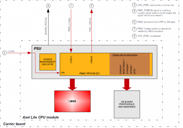
AXEL Lite SOM simplifies this task by embedding all the needed circuitry. The following picture shows a simplified block diagram of PSU/voltage monitoring circuitry:
The PSU is composed of two main blocks:
- power management integrated circuit
- additional generic power management circuitry that completes PMIC functionalities
The PSU:
- generates the proper power-up sequence required by the SOC processor and surrounding memories and peripherals
- synchronizes the powering up of carrier board in order to prevent back power
- provides some spare regulated voltages that can be used to power carrier board devices
Power-up sequence[edit | edit source]
The typical power-up sequence is the following:
- (optional) PMIC_LICELL is powered
- 3.3VIN main power supply rail is powered
- CPU_PORn (active-low) is driven low
- PMIC activates PMIC_VSNVS power output
- PMIC_PWRON signal is pulled-up (unless carrier board circuitry keeps this signal low for any reason)
- PMIC transitions from OFF to ON state
- PMIC initiates power-up sequence needed by MX6 processor
- BOARD_PGOOD signal is raised; this active-high signal indicates that SoM's I/O is powered. This signal can be used to manage carrier board power up sequence in order to prevent back powering (from SoM to carrier board or vice versa). For additional information, please refer to the Note below.
- CPU_PORn is released
Note on BOARD_PGOOD usage[edit | edit source]
BOARD_PGOOD is generally used on carrier board to drive loads such as DC/DC enable inputs or switch on/off control signals.
Depending on the kind of such loads, BOARD_PGOOD might not be able to drive them properly. In these cases a simple 2-input AND port can be used to address this issue. The following picture depicts a principle schematic showing this solution.
VDD_SOM denotes the power rail used to power AXEL Lite SoM.
Real-time clock (RTC) powering[edit | edit source]
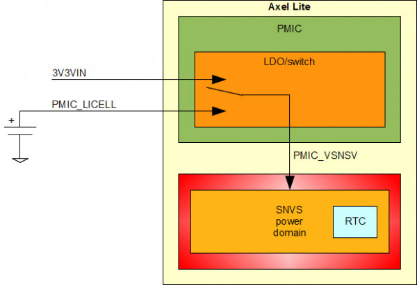
Real-time clock is integrated in iMX6 processor. As such, it belongs to SNVS power domain. This domain, in turn, is powered by PMIC, via PMIC_VSNSV rail (see also this page). PMIC integrates a sort of switch. When 3V3VIN voltage is applied, this is used to power SNVS domain. Otherwise energy is drawn from coin cell battery - if any - connected to PMIC_LICELL (for more details please refer to [1]).
It is worth remembering that 3.0V lithium batteries are supported and that PMIC_VSNSV voltage range is 2.4 - 3.6V. When Axel Lite enters RTC mode and 3V3VIN voltage is removed, typical current absorption from PMIC_LICELL pin is about 135uA. This value is relatively high with respect to the typical lithium coin cell battery capacity (10 - 50mAh). It is recommended that system integrator verify that expected battery lifetime satisfies system requirement. If not, the use of an external low-power RTC device should be considered.
Reset scheme and control signals[edit | edit source]
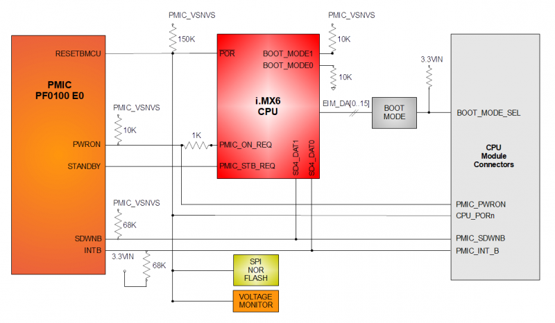
The following picture shows the simplified block diagram of reset scheme and voltage monitoring.
PMIC_VSNVS[edit | edit source]
Some signals that are related to reset circuitry are pulled-up to PMIC_VSNVS. This voltage is generated by PMIC PF0100's VSNVS LDO/Switch and its actual value depends on:
- voltage applied to PMICS's VIN pin
- in case of AxelLite this pin is connected to 3.3VIN power rail
- voltage applied to PMICS's LICELL pin
- in case of AxelLite this pin is connected to pin 14 of SODIMM connector (PMIC_LICELL)
- PMIC's VSNVSCTL register configuration.
Hence it is recommended that system designer takes into account these factors in order to properly manage these signals at carrier board level.
For more details please refer to section VSNVS LDO/Switch of MMPF0100 Advance Information document.
CPU_PORn[edit | edit source]
The following devices can assert this active-low signal:
- PMIC
- multiple-voltage monitor: this device monitors critical power voltages and triggers a reset pulse in case any of these exhibits a brownout condition
Since SPI NOR flash can be used as boot device, CPU_PORn is connected to this device too. This guarantees it is in a known state when reset signal is released.
Handling CPU-initiated software reset[edit | edit source]
By default, MX6 processor does not assert any external signal when it initiates a software reset sequence. Also default software reset implementation does not guarantee that all processor registers are reset properly.
For these reasons, it is strongly recommended to use a different approach that, in combination with the use of a processor's watchdog timer (WDT), provides a full hardware reset in case a software reset is issued.
This technique is implemented in DESK-MX6-L. At software level, U-Boot and Linux kernel software reset routines make use of processor's WDT #2 to assert the WDOG2_B reset signal. This signal in turn is routed to GPIO_1 pad (MUX mode = 1). At hardware level, this signal is AC-coupled to a 3-state output buffer (please refer to U46 chip of AXEL Lite Evaluation_Kit carrier board), driving PMIC_PWRON.
System boot[edit | edit source]
The boot process begins at Power On Reset (POR) where the hardware reset logic forces the ARM core to begin execution starting from the on-chip boot ROM. The boot ROM:
- determines whether the boot is secure or non-secure
- performs some initialization of the system and clean-ups
- reads the mode pins to determine the primary boot device
- once it is satisfied, it executes the boot code
Boot options[edit | edit source]
Two options are available related to system boot. They are identified by the Boot field of the ordering code as follows:
- Boot field = 0 (SOM code: DXLxxxx0xxR): "SPI NOR / SD" option
- Boot field = 1 (SOM code: DXLxxxx1xxR): "NAND / SD" option
For both options, the selection of the primary boot device is determined by the BOOT_MODE_SEL signal as described in the following sections. BOOT_MODE_SEL is latched when processor reset is released.
In any case, boot process is managed by on-chip boot ROM code that is described in detail in processor's Reference Manual.
SPI NOR / SD option[edit | edit source]
Selection of primary boot device is determined by the BOOT_MODE_SEL signal as follows:
- BOOT_MODE_SEL = 0
- primary boot device is SD1
- boot ROM will try to boot a valid image from the SD card first, and then from the SPI NOR. In case no valid image is found, boot ROM shall enable USB serial download mode automatically
- BOOT_MODE_SEL = 1 or floating
- primary boot device is SPI NOR flash connected to eCSPI1
- in case no valid image is found in NOR flash, boot ROM shall enable USB serial download mode automatically
NAND / SD option[edit | edit source]
Selection of primary boot device is determined by the BOOT_MODE_SEL signal as follows:
- BOOT_MODE_SEL = 0
- primary boot device is SD1
- in case no valid image is found in SD card, boot ROM shall enable USB serial download mode automatically
- BOOT_MODE_SEL = 1 or floating
- primary boot device is NAND flash
- in case no valid image is found in NAND flash, boot ROM shall enable USB serial download mode automatically
Important note for DualLite/Solo based products (manufacture mode management)[edit | edit source]
When Dual Lite or Solo processor are used, GPIO_1 and GPIO_4 signals need to be kept high during bootstrap stage in order to prevent the intervention of bootrom's manufacture mode. Bootstrap stage has to be intended as the time elapsing between the release of hardware reset (CPU_PORn) and the execution of the first instruction of user code (typically this is the reset vector of U-Boot boot loader). Please note that, in case GPIO_1 signal is used to implement software reset circuit, it is high during bootstrap stage by design.
On board JTAG connector[edit | edit source]
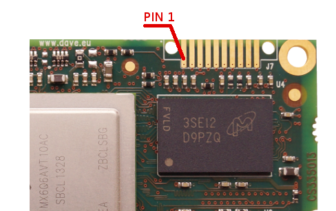
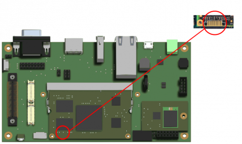
JTAG signals are routed to a dedicated connector on the AXEL Lite PCB.
The connector is placed on the top side of the PCB, at the upper-right corner (please see the picture below).
J7 - SOM Connector's pinout[edit | edit source]
J7 footprint mates with Samtec FSI-110-03-G-S connector. The following table reports the connector's pinout:
| Pin# | Pin name | Function | ARM-20 JTAG | Notes |
|---|---|---|---|---|
| 1 | DGND | - | 4,6,8,10,12,14,16,18,20 | For example documented on Lauterbach specification |
| 2 | JTAG_TCK | - | 9 | - |
| 3 | JTAG_TMS | - | 7 | 10K pull-up to 3V3 (BOARD_PGOOD driven signal) |
| 4 | JTAG_TDO | - | 13 | 10K pull-up to 3V3 (BOARD_PGOOD driven signal) |
| 5 | JTAG_TDI | - | 5 | 10K pull-up to 3V3 (BOARD_PGOOD driven signal) |
| 6 | JTAG_nTRST | - | 3 (*) | 10K pull-up to 3V3 (BOARD_PGOOD driven signal) |
| 7 | CPU_PORn | - | 15 (*) | - |
| 8 | N.C. | - | - | |
| 9 | N.C. | - | - | |
| 10 | JTAG_VREF | - | 1 | 3V3 (BOARD_PGOOD driven signal) |
(*) keep the possibility to be unconnected
Peripherals[edit | edit source]
Peripheral Audio[edit | edit source]
The Audio interface available on AXEL Lite is based on i.MX6 SoC which provides the following subsystems characteristics:
- Audio codecs are provided by SW, which runs on ARM core, supporting (but not limited to) MP3, WMA, AAC, HE-AAC and Pro10
- 3x SSIs
- ESAI (Enhanced Serial Audio Interface)
- SPDIF Tx/Rx
- Audmux
- Audio sample rate conversion accelerator (ASRC)
Description[edit | edit source]
The i.MX6 processor provides SSI Synchronous Serial Interface port that allow to communicate with audio codecs that implement the inter-IC sound bus standard (I2S).
The SSI includes the following features:
- Independent (asynchronous) or shared (synchronous) transmit and receive sections with separate or shared internal/external clocks and frame syncs, operating in Master or Slave mode
- Normal mode operation using frame sync
- 2 sets of Transmit and Receive FIFOs. Each of the four FIFOs is 15x32 bits. The two sets of Tx/Rx FIFOs can be used in Network mode to provide 2 independent channels for transmission and reception (this mode is named as two-channel mode in the following descriptions)
- Programmable data interface modes such as I2S, LSB, MSB aligned
- Programmable word length (8, 10, 12, 16, 18, 20, 22 or 24 bits)
- Programmable I2S modes (Master, Slave or Normal). Maximum audio sampling rate is 196kHz. (Note that maximum sampling rate depends on IPG frequency). Minimum audio sampling rate is 8kHz. Network clock (as an oversampling clock to external device) available as output from SRCK in I2S Master mode
- AC97 support. Max frame rate is 48kHz. Min frame rate is 8kHz
The processor also provides standard Sony/Philips Digital Interface (SPDIF) stereo transceiver that allows the processor to receive and transmit digital audio.
Pin mapping[edit | edit source]
The Pin mapping is described in the Pinout table section
Peripheral CAN[edit | edit source]
AXEL Lite SOM provides two CAN interfaces (FLEXCAN1 and FLEXCAN2) for supporting distributed realtime control with a high level of reliability.
Description[edit | edit source]
The CAN interface available on AXEL Lite is based on i.MX6 FLEXCAN which is a full implementation of the CAN protocol specification, which supports both standard and extended message frames.
The FLEXCAN module implements:
- the CAN protocol version 2.0B
- Standard data and remote frames
- Extended data and remote frames
- Zero to eight bytes data length
- Programmable bit rate up to 1 Mb/sec
- Content-related addressing
- 64 Message Buffers
Pin mapping[edit | edit source]
The Pin mapping is described in the Pinout table section
Peripheral Ethernet[edit | edit source]
The AXEL Lite i.MX6 SOC ENET implements a triple-speed 10/100/1000/1000-Mbit/s ethernet MAC interface.
Description[edit | edit source]
The Ethernet interface available on AXEL Lite is based on i.MX6 ethrnet MAC and ax external ethernet PHY.
The Ethernet MAC supports the following standards and features:
- compliant with the IEEE802.3-2002 standard
- compatibility with half- or full-duplex 10/100-Mbit/s and full-duplex gigabit1 Ethernet LANs
- compliant with the AMD magic packet detection with interrupt for node remote power management
- hardware acceleration block to optimize the performance of network controllers providing TCP/IP, UDP, and ICMP protocol services
Known limitations[edit | edit source]
According to i.MX6 chip errata ERR004512, the ethernet performances are limited to 470Mbps:
ERR004512 ENET: 1 Gb Ethernet MAC (ENET) system limitation

Description:
The theoretical maximum performance of 1 Gbps ENET is limited to 470 Mbps (total for Tx and Rx). The actual measured performance in an optimized environment is up to 400 Mbps.

Projected Impact:Minor.
Limitation of ENET throughput to around 400 Mbps. ENET remains fully compatible to 1Gb standard in terms of protocol and physical signaling. If the TX and RX peak data rate is higher than 400 Mbps, there is a risk of ENET RX FIFO overrun
Pin mapping[edit | edit source]
The Pin mapping is described in the Pinout table section
Peripheral HDMI[edit | edit source]
HDMI (High-Definition Multimedia Interface) is a compact audio/video interface for transmitting uncompressed digital video data and uncompressed/compressed digital audio data.
HDMI connects digital audio/video sources-such as set-top boxes, Blu-ray Disc players, personal computers (PCs), video game consoles, and AV receivers to compatible digital audio devices, computer monitors, and digital televisions.
Description[edit | edit source]
The HDMI interface available on AXEL Lite is based on i.MX6 SoC.
The HDMI port supports the following standards and features:
- High-Definition Multimedia Interface Specification Version 1.4a
- Support for up to 1080p at 60Hz and 720p/1080i at 120Hz HDTV display resolutions
- Support 3D video mode up to 270MHz
Pin mapping[edit | edit source]
The Pin mapping is described in the Pinout table section
Peripheral LVDS[edit | edit source]
The LVDS Display Bridge (LDB) connects the IPU (Image Processing Unit) to an External LVDS Display Interface.
The purpose of the LDB is to support flow of synchronous RGB data from the IPU to external display devices through the LVDS interface.
This support covers all aspects of these activities:
- Connectivity to relevant devices - Displays with LVDS receivers
- Arranging the data as required by the external display receiver and by LVDS display standards
- Synchronization and control capabilities
Description[edit | edit source]
The LVDS interface available on AXEL Lite is based on i.MX6 SoC and provides two LVDS interfaces.
The LVDS ports may be used as follows:
- Single channel output
- Dual channel output (one input source, two channels outputs for two displays)
- Split channel output (one input source, splitted to 2 channels on output)
- Separate 2 channel output (2 input sources from IPU)
The output LVDS port complies to the EIA-644-A standard.
Pin mapping[edit | edit source]
The Pin mapping is described in the Pinout table section
Peripheral MIPI[edit | edit source]
The CSI-2 Host Controller is a digital core that implements all protocol functions defined in the MIPI CSI-2 Specification, providing an interface between the System and the MIPI D-PHY, allowing the communication with a MIPI CSI-2 compliant Camera Sensor
Description[edit | edit source]
The MIPI interface available on AXEL Lite is based on i.MX6 SoC and support the following features:
- Compliant with MIPI Alliance Standard for Camera Serial Interface 2 (CSI-2), Version 1.00 - 29 November 2005
- Interface with MIPI D-PHY following PHY Protocol Interface (PPI), as defined in MIPI Alliance Specification for D-PHY, Version 1.00.00 - 14 May 2009
- Supports up to 2 (S/DL) and 4 (D/Q) D-PHY Rx Data Lanes
- Dynamically configurable multi-lane merging
- Long and Short packet decoding
- Timing accurate signaling of Frame and Line synchronization packets
- Support for several frame formats such as:
- General Frame or Digital Interlaced Video with or without accurate sync timing
- Data type (Packet or Frame level) and Virtual Channel interleaving
- 32-bit Image Data Interface delivering data formatted as recommended in CSI-2 Specification
- Supports all primary and secondary data formats:
- RGB, YUV and RAW color space definitions
- From 24-bit down to 6-bit per pixel
- Generic or user-defined byte-based data types
- Error detection and correction: PHY, Packet, Line, Frame
Camera ports[edit | edit source]
The MIPI CSI-2 Serial port supports the following standards and features:
i.MX 6Solo/6DualLite[edit | edit source]
- Supporting from 80 Mbps to 1 Gbps speed per data lane
- CSI-2 Receiver core can manage one clock lane and up to two lanes
i.MX 6Dual/6Quad[edit | edit source]
- Support up to 1Gbps per lane in 1/2/3-lane mode and up to 800 Mbps/lane in 4-lane mode
- CSI-2 Receiver core can manage one clock lane and up to four data lanes
Pin mapping[edit | edit source]
The Pin mapping is described in the Pinout table section
Peripheral SDIO[edit | edit source]
AXEL Lite SOM provides up to three SDIO interfaces; due to PINMUX restrcitions and usa of the NAND controller onboard, a typical usage on AXEL Lite SOM is the following one:
- SD1 configured in 4-bit mode and used as boot device (with BOOT_SEL)
- SD2 configured in 4-bit mode
- SD3 configured in 8-bit mode: a typical connection for this interface is forx interfacing an external eMMC storage device
Description[edit | edit source]
The SDIO interface available on AXEL Lite is based on i.Mx6 SoC.
The SDIO port supports the following standards and features:
- 1-bit or 4-bit transfer mode specifications for SD and SDIO cards up to UHS-I SDR-104 mode (104 MB/s max)
- 1-bit, 4-bit, or 8-bit transfer mode specifications for MMC cards up to 52 MHz in both SDR and DDR modes (104 MB/s max)
- Compatible with SD Memory, miniSD Memory, SDIO, miniSDIO, SD Combo, MMC and MMC RS, embedded MMC and embedded SD cards
- Up to 200 Mbps data transfer for SD/SDIO cards using 4 parallel data lines
- Up to 416 Mbps data transfer for MMC cards using 8 parallel data lines
- Up to 832 Mbps data transfer for MMC/SD cards using 8 parallel data lines in DDR mode
- Dual internal 32x32-bit FIFOs
Pin mapping[edit | edit source]
The Pin mapping is described in the Pinout table section
Peripheral UART[edit | edit source]
Universal Asynchronous Receiver/Transmitter (UART) provides serial communication capability with external devices through a level converter like RS-232 or RS-485.
Description[edit | edit source]
The UART interface available on AXEL Lite is based on i.MX6 SoC.
The UART ports support the following standards and features:
- One of the five UARTs (UART1) supports 8-wire while others four supports 4-wire
- High-speed TIA/EIA-232-F compatible, up to 4.0 Mbit/s
- Serial IR interface low-speed, IrDA-compatible (up to 115.2 Kbit/s)
- 9-bit or Multidrop mode (RS-485) support (automatic slave address detection)
- 7 or 8 data bits for RS-232 characters, or 9 bit RS-485 format
- 1 or 2 stop bits
- Programmable parity (even, odd, and no parity)
- Hardware flow control support for request to send (RTS_B) and clear to send (CTS_B) signals
- RS-485 driver direction control via CTS_B signal
- Auto baud rate detection (up to 115.2 Kbit/s)
- Two independent, 32-entry FIFOs for transmit and receive
Pin mapping[edit | edit source]
The Pin mapping is described in the Pinout table section
Peripheral USB host[edit | edit source]
Universal Serial Bus (USB) is an industry standard that establishes specifications for cables and connectors and protocols for connection, communication and power supply (interfacing) between computers, peripherals and other computers.
The USB controller block provides high performance USB functionality that conforms to the Universal Serial Bus Specification, Rev. 2.0
Description[edit | edit source]
The two USB interface available on AXEL Lite are based on iMX6 SoC. The USB1 port is connected to the USB 2.0 Controller Core 1 which is a High-Speed/Full-Speed/Low-Speed Host-Only core.
The USB1 host port support the following standards and features:
- USB 2.0 (480 Mbps)
- HS host with integrated High Speed Phy
Pin mapping[edit | edit source]
The Pin mapping is described in the Pinout table section
Peripheral USB OTG[edit | edit source]
Universal Serial Bus (USB) is an industry standard that establishes specifications for cables and connectors and protocols for connection, communication and power supply (interfacing) between computers, peripherals and other computers.
The USB controller block provides high performance USB functionality that conforms to the Universal Serial Bus Specification, Rev. 2.0
Description[edit | edit source]
The two USB interface available on AXEL Lite are based on iMX6 SoC. The USB2 port is connected to the USB 2.0 Controller Core 0 which is an OTG controller core that can operate in Host mode and Device (Peripheral) mode
The USB2 host port support the following standards and features:
- USB 2.0 (480 Mbps)
- HS host with integrated High Speed Phy
- Hardware support for OTG signaling, session request protocol, and host negotiation protocol
- Up to 8 bidirectional endpoints
Pin mapping[edit | edit source]
The Pin mapping is described in the Pinout table section
Peripheral PCI Express[edit | edit source]
Description[edit | edit source]
The PCI Express interface available on AXEL Lite is based on i.MX6 SoC and supports the following standards and features:
- PCI Express Base Specification, Revision 2.0 (including legacy 2.5-Gbps support) @ 5.0 Gbps data rate
- PCI Express Base Specification, Revision 1.1 @ 2.5Gbps data rate
PHY features[edit | edit source]
- 5 Gbps data transmission rate
- Integrated PHY includes transmitter, receiver and PLL
- Programmable RX equalization
- 5Gb/s PCIe Gen 2 and 2.5Gb/s PCIe Gen 1.1 test modes
Pin mapping[edit | edit source]
The Pin mapping is described in the Pinout table section
Peripheral GPIO[edit | edit source]
The GPIO general-purpose input/output peripheral provides dedicated general-purpose pins that can be configured as either inputs or outputs.
Description[edit | edit source]
The GPIOs interface available on AXEL Lite is based on i.MX6 SoC.
The GPIO functionality is provided through registers, an edge-detect circuit, and interrupt generation logic.
When configured as an output, it is possible to write to an internal register to control the state driven on the output pin. When configured as an input, it is possible to detect the state of the input by reading the state of an internal register. In addition, the GPIO peripheral can produce CORE interrupts.
Pin mapping[edit | edit source]
The Pin mapping is described in the Pinout table section
Peripheral Real Time Clock[edit | edit source]
Description[edit | edit source]
The Real Time Clock interface available on AXEL Lite is based on NXP MMPF0100 PMIC.
The Real Time Clock is kept operative through the AXEL Lite PMIC_LICELL pin (J2.14): the LICELL pin provides for a connection of a coin cell backup battery or a “super” capacitor.
A small capacitor should be placed from LICELL to ground under all circumstances.
For more information about PMIC RTC functionality, please refer to the MMPF0100 datasheet.
Powering[edit | edit source]
Real-time clock is integrated in iMX6 processor. As such, it belongs to SNVS power domain. This domain, in turn, is powered by PMIC, via PMIC_VSNSV rail (see also this page). PMIC integrates a sort of switch. When 3V3VIN voltage is applied, this is used to power SNVS domain. Otherwise energy is drawn from coin cell battery - if any - connected to PMIC_LICELL (for more details please refer to [1]).
It is worth remembering that 3.0V lithium batteries are supported and that PMIC_VSNSV voltage range is 2.4 - 3.6V. When AXEL Lite enters RTC mode and 3V3VIN voltage is removed, typical current absorption from PMIC_LICELL pin is about 135uA. This value is relatively high with respect to the typical lithium coin cell battery capacity (10 - 50mAh). It is recommended that system integrator verify that expected battery lifetime satisfies system requirement. If not, the use of an external low-power RTC device should be considered.
Pin mapping[edit | edit source]
The Pin mapping is described in the Pinout table section
Peripheral Watchdog[edit | edit source]
The Watchdog Timer (WDOG) protects against system failures by providing a method by which to escape from unexpected events or programming errors.
Description[edit | edit source]
By default, the Watchdog Timer of iMX6 SOC is internally used on AXEL Lite for the CPU-initiated software reset function.
For more details see the reset scheme and control signals section.
The Watchdog timer supports the following features:
- Configurable timeout counter with timeout periods from 0.5 to 128 seconds which, after timeout expiration, result in the assertion of WDOG_RESET_B_DEB reset signal
- Time resolution of 0.5 seconds
- Power down counter with fixed timeout period of 16 seconds, which if not disabled after reset will assert WDOG_B signal low
Pin mapping[edit | edit source]
The Pin mapping is described in the Pinout table section
Electrical, Thermal and Mechanical Features[edit | edit source]
Operational characteristics[edit | edit source]
Maximum ratings[edit | edit source]
| Parameter | Min | Typ | Max | Unit |
|---|---|---|---|---|
| Main power supply voltage | -0.3 | 3.3 | 3.6 | V |
Recommended ratings[edit | edit source]
| Parameter | Min | Typ | Max | Unit |
|---|---|---|---|---|
| Main power supply voltage | 3.135 | 3.3 | 3.465 | V |
Power consumption[edit | edit source]
Providing theoretical maximum power consumption value would be useless for the majority of system designers building their application upon AXEL Lite module. Practically speaking, these figures would be of no help when it comes to size power supply unit or to perform thermal design of real systems.
Instead, several configurations have been tested in order to provide figures that are measured on real-world use cases.
Please note that AXEL Lite platform is so flexible that it is virtually impossible to test for all possible configurations and applications on the market. The use cases here presented should cover most of real-world scenarios. However actual customer's application might require more power than values reported here or customer's use case may be differ significantly with respect to the ones here considered.
Therefore, application-specific requirements have always to be taken into consideration in order to size power supply unit and to implement thermal management properly.
Use cases results[edit | edit source]
Measurements have been performed on the AXEL Lite SOM under test is equipped with:
- i.MX6 DualLite (p.n. MCIMX6U7CVM08AC)
- 1 GB DDR3L SDRAM
- 1 GB NAND
1 Gbps Ethernet link has been always active during the test.
The table below reports the power consumption measurements for the considered use cases.
| Checkpoint | Power (mW) |
|---|---|
| U-boot prompt | 2370 |
| Linux prompt | 1610 |
| Stress App test (*) | 5915 |
(*) Stressful Application Test: https://github.com/stressapptest/stressapptest
Thermal management[edit | edit source]
The AXEL Lite SOM is designed to support the maximum available temperature range declared by the manufacturer.
The customer shall define and conduct a reasonable number of tests and verification in order to qualify the DUT capabilities to manage the heat dissipation.
Any heatsink, fan etc shall be defined case by case.
DAVE Embedded Systems' team is available for any additional information, please contact sales@dave.eu.
Software thermal protection[edit | edit source]
In DESK-MX6-L, two software thermal protection mechanisms are implemented. Both are based on the processor's temperature sensor. It is worth remembering that maximum junction temperature (also denoted as Tj in the rest of the document) is:
- 95°C for commercial parts
- 105°C for extended commercial and industrial parts
- 125°C for automotive parts.
U-Boot[edit | edit source]
At U-Boot level, automatic boot procedure is halted until Tj is smaller than (following temperatures might seem excessively low but they take into account the intrinsic poor precision of the temperature sensor to provide a reasonable safe margin):
- 80°C for commercial parts
- 90 for extended commercial and industrial parts
- 110°C for automotive parts.
Linux kernel[edit | edit source]
At Linux level, a more sophisticated protection mechanism is implemented. Please refer to the following sections for more details.
The default temperature thresholds depend on the silicon grade, as follows:
- for commercial parts
- passive threshold: 85°C
- critical threshold: 90°C
- for extended commercial and industrial parts
- passive threshold: 95°C
- critical threshold: 100°C
- for automotive parts
- passive threshold: 115°C
- critical threshold: 120°C.
Practically speaking, for DESK-MX6-L this mechanism makes use of two different thresholds, denoted as trip_point0 (also known as passive threshold) and trip_point1 (also known as critical threshold.
When Tj reaches trip_point0, Linux kernel scales down processor frequency:
System is too hot. GPU3D will work at 1/64 clock.
If Tj reaches trip_point1, a complete shutdown is triggered:
thermal thermal_zone0: critical temperature reached(100 C),shutting down
By default, temperature thresholds are set up as follows:
trip_point0: 85°Ctrip_point1: 100°C.
Trip point thresholds can be accessed via sysfs interface from user space. The following example shows how to read the values of the trip points:
root@axel-lite:~# cat /sys/devices/virtual/thermal/thermal_zone0/trip_point_0_temp
85000
root@axel-lite:~# cat /sys/devices/virtual/thermal/thermal_zone0/trip_point_1_temp
100000
This example shows how to set trip points 0 and 1 to 95°C and 100°C respectively:
echo 95000 > /sys/class/thermal/thermal_zone0/trip_point_0_temp
echo 100000 > /sys/class/thermal/thermal_zone0/trip_point_1_temp
|
Please note that
|
To read current processor temperature please issue this command (reported temperature is 36.676°C in the example):
root@axel-lite:~# cat /sys/class/thermal/thermal_zone0/temp
36676
For more details about this functionality, please refer to Documentation/thermal/sysfs-api.txt in the kernel sources.
Mechanical specifications[edit | edit source]
This chapter describes the mechanical characteristics of the AXEL Lite module.
Board Layout[edit | edit source]
The following figure shows the physical dimensions of the AXEL Lite module:
Connectors[edit | edit source]
The following figure shows the AXEL Lite connector layout:
CAD drawings[edit | edit source]
3D drawings[edit | edit source]
