BORA Lite SOM/BORA Lite Hardware/pdf
General Information[edit | edit source]
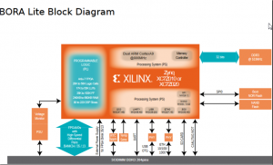
BORA Lite Block Diagram[edit | edit source]
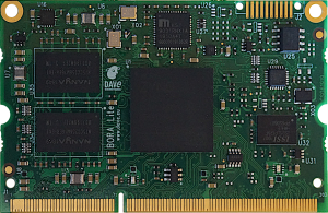
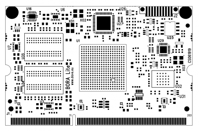
BORA Lite TOP View[edit | edit source]
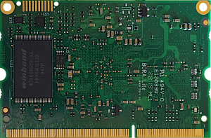
BORA Lite BOTTOM View[edit | edit source]
Processor and memory subsystem[edit | edit source]
The heart of BORA Lite module is composed of the following components:
- Xilinx Zynq XC7Z007S/012S/014S single core ARM Cortex-A9 or XC7Z010/XC7Z020 dual core ARM Cortex-A9 MPCore
- Power supply unit
- DDR memory banks
- NOR and NAND flash banks
- 204 SO-DIMM connector with interfaces signals
This chapter shortly describes the main BORA Lite components.
Processor Info[edit | edit source]
The Zynq™-7000 family is based on the Xilinx Extensible Processing Platform (EPP) architecture. These products integrate a feature-rich single/dual core ARM® Cortex™-A9 based processing system (PS) and 28 nm Xilinx programmable logic (PL) in a single device. The ARM Cortex-A9 CPUs are the heart of the PS and also include on-chip memory, external memory interfaces, and a rich set of peripheral connectivity interfaces. The Zynq-7000 family offers the flexibility and scalability of an FPGA, while providing performance, power, and ease of use typically associated with ASIC and ASSPs. The range of devices in the Zynq-7000 AP SoC family enables designers to target cost-sensitive as well as high-performance applications from a single platform using industry-standard tools. While each device in the Zynq-7000 family contains the same PS, the PL and I/O resources vary between the devices. As a result, the Zynq-7000 AP SoC devices are able to serve a wide range of applications including:
- Automotive driver assistance, driver information, and infotainment
- Broadcast camera
- Industrial motor control, industrial networking, and machine vision
- IP and Smart camera
- LTE radio and baseband
- Medical diagnostics and imaging
- Multifunction printers
- Video and night vision equipment
The processors in the PS always boot first, allowing a software centric approach for PL system boot and PL configuration. The PL can be configured as part of the boot process or configured at some point in the future. Additionally, the PL can be completely reconfigured or used with partial, dynamic reconfiguration (PR). PR allows configuration of a portion of the PL. This enables optional design changes such as updating coefficients or time-multiplexing of the PL resources by swapping in new algorithms as needed.
Bora can mount two versions of the Zynq processor. The following table shows a comparison between the processor models, highlighting the differences:
| Processor | Programmable logic cells | LUTs | Flip flops | Extensible block RAM | DSP slices | Peak DSP performance |
| XC7Z007S | 23K Logic Cells | 14400 | 28800 | 1.8 Mb | 66 | 73 GMACs |
| XC7Z012S | 55K Logic Cells | 34400 | 68800 | 2.5 Mb | 120 | 131 GMACs |
| XC7Z014S | 65K Logic Cells | 40600 | 81200 | 3.8Mb | 170 | 187 GMACs |
| XC7Z010 | 28K Logic Cells | 17600 | 35200 | 2.1 Mb | 80 | 100 GMACs |
| XC7Z020 | 85K Logic Cells | 53200 | 106400 | 4.9 Mb | 220 | 276 GMACs |
RAM memory bank[edit | edit source]
DDR3 SDRAM memory bank is composed by 2x 16-bit width chips resulting in a 32-bit combined width bank. The following table reports the SDRAM specifications:
| CPU connection | SDRAM bus |
| Size min | 512 MB |
| Size max | 1 GB |
| Width | 32 bit |
| Speed | 533 MHz |
NOR flash bank[edit | edit source]
NOR flash is a Serial Peripheral Interface (SPI) device. By default this device is connected to SPI channel 0 and acts as boot memory. The following table reports the NOR flash specifications:
| CPU connection | SPI Channel 0 |
| Size min | 8 MB |
| Size max | 16 MB - The limitation to max 16MB is due to this Errata from Xilinx. The proposed solution by Xilinx has not been approved by DAVE Embedded Systems |
| Chip select | SPI_CS0n |
| Bootable | Yes |
NAND flash bank[edit | edit source]
On board main storage memory is a 8-bit wide NAND flash. By default it is connected to chip select. The following table reports the NAND flash specifications:
| CPU connection | Static memory controller |
| Page size | 512 byte, 2 kbyte or 4 kbyte |
| Size min | 128 MB |
| Size max | 1 GB |
| Width | 8 bit |
| Chip select | NAND_CS0 |
| Bootable | Yes |
Power supply unit[edit | edit source]
Bora, as the other Ultra Line CPU modules, embeds all the elements required for powering the unit, therefore power sequencing is self-contained and simplified. Nevertheless, power must be provided from carrier board, and therefore users should be aware of the ranges power supply can assume as well as all other parameters. For detailed information, please refer to the Power supply wiki page.
CPU module connectors[edit | edit source]
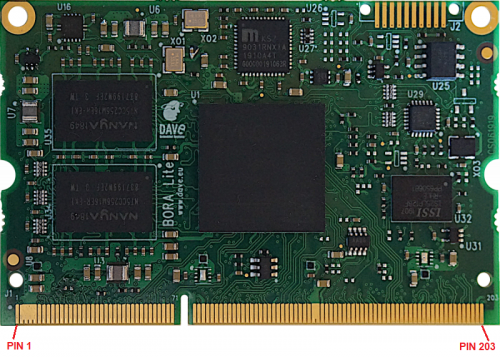
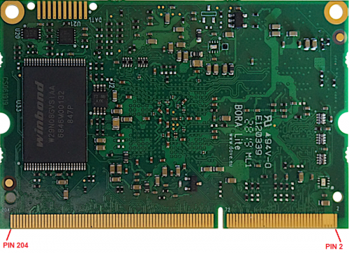
All interface signals Bora provides are routed through a 204 pin DDR3 SO-DIMM edge connector (named J1). The dedicated carrier board must mount the mating connector and connect the desired peripheral interfaces according to BORA Lite pinout specifications.
Hardware versioning and tracking[edit | edit source]
BORA Lite SOM implements well established versioning and tracking mechanisms:
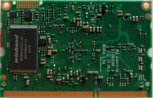
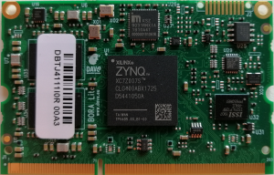
- PCB version is copper printed on PCB itself, as shown in Fig. 1
- serial number: it is printed on a white label, as shown in Fig. 2: see also Product serial number page for more details
- ConfigID: it is used by software running on the board for the identification of the product model/hardware configuration. For more details, please refer to this link
- On BORA Lite SOM ConfigID is stored in the internal I2C EEPROM
Processor and memory subsystem[edit | edit source]
The heart of BORA Lite module is composed of the following components:
- Xilinx Zynq XC7Z007S/012S/014S single core ARM Cortex-A9 or XC7Z010/XC7Z020 dual core ARM Cortex-A9 MPCore
- Power supply unit
- DDR memory banks
- NOR and NAND flash banks
- 204 SO-DIMM connector with interfaces signals
This chapter shortly describes the main BORA Lite components.
Processor Info[edit | edit source]
The Zynq™-7000 family is based on the Xilinx Extensible Processing Platform (EPP) architecture. These products integrate a feature-rich single/dual core ARM® Cortex™-A9 based processing system (PS) and 28 nm Xilinx programmable logic (PL) in a single device. The ARM Cortex-A9 CPUs are the heart of the PS and also include on-chip memory, external memory interfaces, and a rich set of peripheral connectivity interfaces. The Zynq-7000 family offers the flexibility and scalability of an FPGA, while providing performance, power, and ease of use typically associated with ASIC and ASSPs. The range of devices in the Zynq-7000 AP SoC family enables designers to target cost-sensitive as well as high-performance applications from a single platform using industry-standard tools. While each device in the Zynq-7000 family contains the same PS, the PL and I/O resources vary between the devices. As a result, the Zynq-7000 AP SoC devices are able to serve a wide range of applications including:
- Automotive driver assistance, driver information, and infotainment
- Broadcast camera
- Industrial motor control, industrial networking, and machine vision
- IP and Smart camera
- LTE radio and baseband
- Medical diagnostics and imaging
- Multifunction printers
- Video and night vision equipment
The processors in the PS always boot first, allowing a software centric approach for PL system boot and PL configuration. The PL can be configured as part of the boot process or configured at some point in the future. Additionally, the PL can be completely reconfigured or used with partial, dynamic reconfiguration (PR). PR allows configuration of a portion of the PL. This enables optional design changes such as updating coefficients or time-multiplexing of the PL resources by swapping in new algorithms as needed.
Bora can mount two versions of the Zynq processor. The following table shows a comparison between the processor models, highlighting the differences:
| Processor | Programmable logic cells | LUTs | Flip flops | Extensible block RAM | DSP slices | Peak DSP performance |
| XC7Z007S | 23K Logic Cells | 14400 | 28800 | 1.8 Mb | 66 | 73 GMACs |
| XC7Z012S | 55K Logic Cells | 34400 | 68800 | 2.5 Mb | 120 | 131 GMACs |
| XC7Z014S | 65K Logic Cells | 40600 | 81200 | 3.8Mb | 170 | 187 GMACs |
| XC7Z010 | 28K Logic Cells | 17600 | 35200 | 2.1 Mb | 80 | 100 GMACs |
| XC7Z020 | 85K Logic Cells | 53200 | 106400 | 4.9 Mb | 220 | 276 GMACs |
RAM memory bank[edit | edit source]
DDR3 SDRAM memory bank is composed by 2x 16-bit width chips resulting in a 32-bit combined width bank. The following table reports the SDRAM specifications:
| CPU connection | SDRAM bus |
| Size min | 512 MB |
| Size max | 1 GB |
| Width | 32 bit |
| Speed | 533 MHz |
NOR flash bank[edit | edit source]
NOR flash is a Serial Peripheral Interface (SPI) device. By default this device is connected to SPI channel 0 and acts as boot memory. The following table reports the NOR flash specifications:
| CPU connection | SPI Channel 0 |
| Size min | 8 MB |
| Size max | 16 MB - The limitation to max 16MB is due to this Errata from Xilinx. The proposed solution by Xilinx has not been approved by DAVE Embedded Systems |
| Chip select | SPI_CS0n |
| Bootable | Yes |
NAND flash bank[edit | edit source]
On board main storage memory is a 8-bit wide NAND flash. By default it is connected to chip select. The following table reports the NAND flash specifications:
| CPU connection | Static memory controller |
| Page size | 512 byte, 2 kbyte or 4 kbyte |
| Size min | 128 MB |
| Size max | 1 GB |
| Width | 8 bit |
| Chip select | NAND_CS0 |
| Bootable | Yes |
Power supply unit[edit | edit source]
Bora, as the other Ultra Line CPU modules, embeds all the elements required for powering the unit, therefore power sequencing is self-contained and simplified. Nevertheless, power must be provided from carrier board, and therefore users should be aware of the ranges power supply can assume as well as all other parameters. For detailed information, please refer to the Power supply wiki page.
CPU module connectors[edit | edit source]
All interface signals Bora provides are routed through a 204 pin DDR3 SO-DIMM edge connector (named J1). The dedicated carrier board must mount the mating connector and connect the desired peripheral interfaces according to BORA Lite pinout specifications.
Part number composition[edit | edit source]
BORA Lite SOM module part number is identified by the following digit-code table:
| Part number structure | Options | Description |
|---|---|---|
| Family | DBT | Family prefix code |
| SOC |
|
System on chip definition (and FPGA speed grade) |
| NOR SPI |
|
QUAD SPI NOR flash memory size - The limitation to max 16MB is due to this Errata from Xilinx. The proposed solution by Xilinx has not been approved by DAVE Embedded Systems |
| RAM |
|
DDR3 Memory RAM size |
| NAND |
|
Flash memory NAND size |
| Boot/Misc |
|
Boot options |
| Temperature range |
|
For the DAVE Embedded Systems' product Temperature Range classification, please find more information at the page Products Classification |
| PCB revision |
|
PCB release may change for manufacturing purposes (i.e. text fixture adaptation) |
| Manufacturing option |
|
typically connected to production process and quality |
| Software Configuration | -00: standard factory u-boot pre-programmed
-XX: custom version |
If customers require custom SW deployed this section should be defined and agreed. Please contact technical support |
Example[edit | edit source]
BORA Lite SOM code DBTD4111I0R-00
- DBT - BORA Lite SOM module
- D - XC7Z020 ARM Cortex-A9 866MHz - Speed grade -1
- 4 - 16MB NOR Flash
- 1 - 1GB DDR3
- 1 - 1GB NAND flash
- 1 - NOR boot
- I - Industrial temperature range
- 0 - PCB first version
- R- RoHS manufacturing process
- -00 - standard u-boot pre-programmed
Pinout Table[edit | edit source]
Connectors description[edit | edit source]
In the following table are described all available connectors integrated on BORA Lite SOM:
| Connector name | Connector Type | Notes | Carrier board counterpart |
|---|---|---|---|
| J1 | SODIMM DDR3 edge connector 204 pin | TE Connectivity 2-2013289-1 |
The dedicated carrier board must mount the mating connector and connect the desired peripheral interfaces according to BORA Lite pinout specifications. See the images below for reference:
Pinout table naming conventions[edit | edit source]
This chapter contains the pinout description of the BORA Lite SOM, grouped in two tables (odd and even pins) that report the pin mapping of the 204-pin SO-DIMM BORA Lite connector. Each row in the pinout tables contains the following information:
| Pin | Reference to the connector pin |
| Pin Name | Pin (signal) name on the AxelLite connectors |
| Internal connections |
Connections to the components
|
| Ball/pin # | Component ball/pin number connected to signal |
| Voltage | I/O voltage levels |
| Type | Pin type:
|
| Notes | Remarks on special pin characteristics |
SODIMM ODD pins declaration[edit | edit source]
| Pin | Pin Name | Internal Connections | Ball/pin # | Supply Group | Type | Voltage | Note |
| J1.1 | DGND | DGND | n.a. | ||||
| J1.3 | 3.3VIN | +3.3 V | n.a. | ||||
| J1.5 | 3.3VIN | +3.3 V | n.a. | ||||
| J1.7 | 3.3VIN | +3.3 V | n.a. | ||||
| J1.9 | 3.3VIN | +3.3 V | n.a. | ||||
| J1.11 | DGND | DGND | n.a. | ||||
| J1.13 | ETH_LED1 | LAN.LED1 / PME_N1 | 17 | ||||
| J1.15 | ETH_LED2 | LAN.LED2 | 15 | ||||
| J1.17 | DGND | DGND | n.a. | ||||
| J1.19 | ETH_TXRX0_P | LAN.TXRXP_A | 2 | ||||
| J1.21 | ETH_TXRX0_M | LAN.TXRXM_A | 3 | ||||
| J1.23 | ETH_TXRX1_P | LAN.TXRXP_B | 5 | ||||
| J1.25 | ETH_TXRX1_M | LAN.TXRXM_B | 6 | ||||
| J1.27 | ETH_TXRX2_P | LAN.TXRXP_C | 7 | ||||
| J1.29 | ETH_TXRX2_M | LAN.TXRXM_C | 8 | ||||
| J1.31 | ETH_TXRX3_P | LAN.TXRXP_D | 10 | ||||
| J1.33 | ETH_TXRX3_M | LAN.TXRXM_D | 11 | ||||
| J1.35 | DGND | DGND | n.a. | ||||
| J1.37 | PS_MIO40_501 | CPU.PS_MIO40_501 | D14 | ||||
| J1.39 | PS_MIO41_501 | CPU.PS_MIO41_501 | C17 | ||||
| J1.41 | VDDIO_BANK13 | FPGA.VCCO_13 | T8 U11 W7 Y10 |
N.B. Although BANK 13 is not available on Bora Lite SOMs equipped with the XC7Z010 SOC, VDDIO_BANK13 pin must not be left open and must be connected as described in Programmable logic. | |||
| J1.43 | IO_L6N_T0_VREF_13 | FPGA.IO_L6N_T0_VREF_13 | V5 | Not available on Bora Lite SOMs equipped with the XC7Z007S/XC7Z010 SOC | |||
| J1.45 | IO_L22P_T3_13 | FPGA.IO_L22P_T3_13 | V6 | Not available on Bora Lite SOMs equipped with the XC7Z007S/XC7Z010 SOC | |||
| J1.47 | IO_L22N_T3_13 | FPGA.IO_L22N_T3_13 | W6 | Not available on Bora Lite SOMs equipped with the XC7Z007S/XC7Z010 SOC | |||
| J1.49 | IO_L11P_T1_SRCC_13 | FPGA.IO_L11P_T1_SRCC_13 | U7 | Not available on Bora Lite SOMs equipped with the XC7Z007S/XC7Z010 SOC | |||
| J1.51 | IO_L11N_T1_SRCC_13 | FPGA.IO_L11N_T1_SRCC_13 | V7 | Not available on Bora Lite SOMs equipped with the XC7Z007S/XC7Z010 SOC | |||
| J1.53 | IO_L13N_T2_MRCC_13 | FPGA.IO_L13N_T2_MRCC_13 | Y6 | Not available on Bora Lite SOMs equipped with the XC7Z007S/XC7Z010 SOC | |||
| J1.55 | IO_L13P_T2_MRCC_13 | FPGA.IO_L13P_T2_MRCC_13 | Y7 | Not available on Bora Lite SOMs equipped with the XC7Z007S/XC7Z010 SOC | |||
| J1.57 | DGND | DGND | n.a. | ||||
| J1.59 | IO_L15N_T2_DQS_13 | FPGA.IO_L15N_T2_DQS_13 | W8 | Not available on Bora Lite SOMs equipped with the XC7Z007S/XC7Z010 SOC | |||
| J1.61 | IO_L15P_T2_DQS_13 | FPGA.IO_L15P_T2_DQS_13 | V8 | Not available on Bora Lite SOMs equipped with the XC7Z007S/XC7Z010 SOC | |||
| J1.63 | IO_L16P_T2_13 | FPGA.IO_L16P_T2_13 | W10 | Not available on Bora Lite SOMs equipped with the XC7Z007S/XC7Z010 SOC | |||
| J1.65 | IO_L16N_T2_13 | FPGA.IO_L16N_T2_13 | W9 | Not available on Bora Lite SOMs equipped with the XC7Z007S/XC7Z010 SOC | |||
| J1.67 | VDDIO_BANK13 | FPGA.VCCO_13 | T8 U11 W7 Y10 |
N.B. Although BANK 13 is not available on Bora Lite SOMs equipped with the XC7Z010 SOC, VDDIO_BANK13 pin must not be left open and must be connected as described in Programmable logic. | |||
| J1.69 | IO_L14N_T2_SRCC_13 | FPGA.IO_L14N_T2_SRCC_13 | Y8 | Not available on Bora Lite SOMs equipped with the XC7Z007S/XC7Z010 SOC | |||
| J1.71 | IO_L14P_T2_SRCC_13 | FPGA.IO_L14P_T2_SRCC_13 | Y9 | Not available on Bora Lite SOMs equipped with the XC7Z007S/XC7Z010 SOC | |||
| J1.73 | DGND | DGND | n.a. | ||||
| J1.75 | ETH0_PHY_RST | LAN.RESET_N | 41 | Internally connected to PS_MIO51_501 | |||
| J1.77 | VDDIO_BANK34 | FPGA.VCCO_BANK34 | N19 R15 T18 V14 W17 Y20 |
||||
| J1.79 | IO_0_34 | FPGA.IO_0_34 | R19 | ||||
| J1.81 | IO_25_34 | FPGA.IO_25_34 | T19 | Optionally connected to ETH 25MHz OSC ENABLE Optionally connected to USB 26MHz OSC ENABLE | |||
| J1.83 | IO_L8N_T1_34 | FPGA.IO_L8N_T1_34 | Y14 | ||||
| J1.85 | IO_L8P_T1_34 | FPGA.IO_L8P_T1_34 | W14 | ||||
| J1.87 | DGND | DGND | n.a. | ||||
| J1.89 | IO_L7P_T1_34 | FPGA.IO_L7P_T1_34 | Y16 | ||||
| J1.91 | IO_L7N_T1_34 | FPGA.IO_L7N_T1_34 | Y17 | ||||
| J1.93 | IO_L2P_T0_34 | FPGA.IO_L2P_T0_34 | T12 | ||||
| J1.95 | IO_L2N_T0_34 | FPGA.IO_L2N_T0_34 | U12 | ||||
| J1.97 | IO_L4P_T0_34 | FPGA.IO_L4P_T0_34 | V12 | ||||
| J1.99 | IO_L4N_T0_34 | FPGA.IO_L4N_T0_34 | W13 | ||||
| J1.101 | IO_L18P_T2_34 | FPGA.IO_L18P_T2_34 | V16 | ||||
| J1.103 | IO_L18N_T2_34 | FPGA.IO_L18N_T2_34 | W16 | ||||
| J1.105 | IO_L11P_T1_SRCC_34 | FPGA.IO_L11P_T1_SRCC_34 | U14 | ||||
| J1.107 | IO_L11N_T1_SRCC_34 | FPGA.IO_L11N_T1_SRCC_34 | U15 | ||||
| J1.109 | DGND | DGND | n.a. | ||||
| J1.111 | IO_L17P_T2_34 | FPGA.IO_L17P_T2_34 | Y18 | ||||
| J1.113 | IO_L17N_T2_34 | FPGA.IO_L17N_T2_34 | Y19 | ||||
| J1.115 | IO_L16N_T2_34 | FPGA.IO_L16N_T2_34 | W20 | ||||
| J1.117 | IO_L16P_T2_34 | FPGA.IO_L16P_T2_34 | V20 | ||||
| J1.119 | IO_L24P_T3_34 | FPGA.IO_L24P_T3_34 | P15 | ||||
| J1.121 | IO_L24N_T3_34 | FPGA.IO_L24N_T3_34 | P16 | ||||
| J1.123 | IO_L23N_T3_34 | FPGA.IO_L23N_T3_34 | P18 | ||||
| J1.125 | IO_L23P_T3_34 | FPGA.IO_L23P_T3_34 | N17 | ||||
| J1.127 | VDDIO_BANK34 | FPGA.VCCO_BANK34 | N19 R15 T18 V14 W17 Y20 |
||||
| J1.129 | VDDIO_BANK34 | FPGA.VCCO_BANK34 | N19 R15 T18 V14 W17 Y20 |
||||
| J1.131 | DGND | DGND | n.a. | ||||
| J1.133 | IO_L7P_T1_AD2P_35 | FPGA.IO_L7P_T1_AD2P_35 | M19 | ||||
| J1.135 | IO_L7N_T1_AD2N_35 | FPGA.IO_L7N_T1_AD2N_35 | M20 | ||||
| J1.137 | IO_L8N_T1_AD10N_35 | FPGA.IO_L8N_T1_AD10N_35 | M18 | ||||
| J1.139 | IO_L8P_T1_AD10P_35 | FPGA.IO_L8P_T1_AD10P_35 | M17 | ||||
| J1.141 | IO_L11N_T1_SRCC_35 | FPGA.IO_L11N_T1_SRCC_35 | L17 | ||||
| J1.143 | IO_L11P_T1_SRCC_35 | FPGA.IO_L11P_T1_SRCC_35 | L16 | ||||
| J1.145 | IO_L10P_T1_AD11P_35 | FPGA.IO_L10P_T1_AD11P_35 | K19 | ||||
| J1.147 | IO_L10N_T1_AD11N_35 | FPGA.IO_L10N_T1_AD11N_35 | J19 | ||||
| J1.149 | IO_L14P_T2_AD4P_SRCC_35 | FPGA.IO_L14P_T2_AD4P_SRCC_35 | J18 | ||||
| J1.151 | IO_L14N_T2_AD4N_SRCC_35 | FPGA.IO_L14N_T2_AD4N_SRCC_35 | H18 | ||||
| J1.153 | DGND | DGND | n.a. | ||||
| J1.155 | IO_0_35 | FPGA.IO_0_35 | G14 | ||||
| J1.157 | IO_25_35 | FPGA.IO_25_35 | J15 | ||||
| J1.159 | IO_L9P_T1_DQS_AD3P_35 | FPGA.IO_L9P_T1_DQS_AD3P_35 | L19 | ||||
| J1.161 | IO_L9N_T1_DQS_AD3N_35 | FPGA.IO_L9N_T1_DQS_AD3N_35 | L20 | ||||
| J1.163 | IO_L17P_T2_AD5P_35 | FPGA.IO_L17P_T2_AD5P_35 | J20 | ||||
| J1.165 | IO_L17N_T2_AD5N_35 | FPGA.IO_L17N_T2_AD5N_35 | H20 | ||||
| J1.167 | IO_L21P_T3_DQS_AD14P_35 | FPGA.IO_L21P_T3_DQS_AD14P_35 | N15 | ||||
| J1.169 | IO_L21N_T3_DQS_AD14N_35 | FPGA.IO_L21N_T3_DQS_AD14N_35 | N16 | ||||
| J1.171 | IO_L12N_T1_MRCC_35 | FPGA.IO_L12N_T1_MRCC_35 | K18 | ||||
| J1.173 | IO_L12P_T1_MRCC_35 | FPGA.IO_L12P_T1_MRCC_35 | K17 | ||||
| J1.175 | DGND | DGND | n.a. | ||||
| J1.177 | IO_L6N_T0_VREF_35 | FPGA.IO_L6N_T0_VREF_35 | F17 | ||||
| J1.179 | IO_L6P_T0_35 | FPGA.IO_L6P_T0_35 | F16 | ||||
| J1.181 | IO_L19N_T3_VREF_35 | FPGA.IO_L19N_T3_VREF_35 | G15 | ||||
| J1.183 | IO_L19P_T3_35 | FPGA.IO_L19P_T3_35 | H15 | ||||
| J1.185 | IO_L3P_T0_DQS_AD1P_35 | FPGA.IO_L3P_T0_DQS_AD1P_35 | E17 | ||||
| J1.187 | IO_L3N_T0_DQS_AD1N_35 | FPGA.IO_L3N_T0_DQS_AD1N_35 | D18 | ||||
| J1.189 | IO_L13P_T2_MRCC_35 | FPGA.IO_L13P_T2_MRCC_35 | H16 | ||||
| J1.191 | IO_L13N_T2_MRCC_35 | FPGA.IO_L13N_T2_MRCC_35 | H17 | ||||
| J1.193 | IO_L1N_T0_AD0N_35 | FPGA.IO_L1N_T0_AD0N_35 | B20 | ||||
| J1.195 | IO_L1P_T0_AD0P_35 | FPGA.IO_L1P_T0_AD0P_35 | C20 | ||||
| J1.197 | IO_L2P_T0_AD8P_35 | FPGA.IO_L2P_T0_AD8P_35 | B19 | ||||
| J1.199 | IO_L2N_T0_AD8N_35 | FPGA.IO_L2N_T0_AD8N_35 | A20 | ||||
| J1.201 | VDDIO_BANK35 | FPGA.VCCO_35 | C19 F18 H14 J17 K20 M16 |
||||
| J1.203 | DGND | DGND | n.a. |
SODIMM EVEN pins declaration[edit | edit source]
| Pin | Pin Name | Internal Connections | Ball/pin # | Supply Group | Type | Voltage | Note |
| J1.2 | DGND | DGND | n.a. | ||||
| J1.4 | 3.3VIN | +3.3 V | n.a. | ||||
| J1.6 | 3.3VIN | +3.3 V | n.a. | ||||
| J1.8 | 3.3VIN | +3.3 V | n.a. | ||||
| J1.10 | 3.3VIN | +3.3 V | n.a. | ||||
| J1.12 | DGND | DGND | n.a. | ||||
| J1.14 | BOARD_PGOOD | PSUSWITCHFPGABANK13.ON PSUSWITCHFPGABANK500/34.ON PSUSWITCHFPGABANK35.ON PSUSWITCHFPGABANK501.ON DDRVREFREGULATOR.PGOOD |
3 3 3 3 9 |
Open-drain with internal pull-up (10K) to 3.3VIN
For further details, please refer to Power Supply | |||
| J1.16 | CB_PWR_GOOD | 1V0REGULATOR.ENABLE | n.a. | For further details, please refer to Power Supply | |||
| J1.18 | SYS_RSTN | CPU.PS_SRST_B_501 MTR.~RST |
B10 5 |
For further details, please refer to Reset signals | |||
| J1.20 | MRSTN | MTR.MR | 6 | Optionally internally connected to PORSTn (CPU.PS_POR_B_500)
For further details, please refer to Reset signals | |||
| J1.22 | VBAT_BKP | RTC.VBAT | 6 | ||||
| J1.24 | PS_MIO49_501 | CPU.PS_MIO49_501 | C12 | ||||
| J1.26 | PS_MIO48_501 | CPU.PS_MIO48_501 | B12 | ||||
| J1.28 | PS_MIO47_501 | CPU.PS_MIO47_501 | B14 | ||||
| J1.30 | DGND | DGND | n.a. | ||||
| J1.32 | PS_MIO46_501 | CPU.PS_MIO46_501 | D16 | ||||
| J1.34 | PS_MIO45_501 | CPU.PS_MIO45_501 | B15 | ||||
| J1.36 | PS_MIO44_501 | CPU.PS_MIO44_501 | F13 | ||||
| J1.38 | PS_MIO43_501 | CPU.PS_MIO43_501 | A9 | ||||
| J1.40 | PS_MIO42_501 | CPU.PS_MIO42_501 | E12 | ||||
| J1.42 | PS_MIO15_500 | CPU.PS_MIO15_500 WDT.WDI |
C8 1 |
This signal is pulled down by 2.2kOhm resistor See also this page | |||
| J1.44 | SPI0_CS0n | CPU.PS_MIO1_500 | A7 | ||||
| J1.46 | SPI0_DQ0/MODE3/NAND_ALE | CPU.PS_MIO2_500 | B8 | This signal is pulled up or down by 20kOhm resistor to select proper bootstrap configuration. | |||
| J1.48 | SPI0_DQ1/MODE1/NAND_WE | CPU.PS_MIO3_500 | D6 | This signal is pulled up or down by 20kOhm resistor to select proper bootstrap configuration. | |||
| J1.50 | SPI0_DQ2/MODE2/NAND_IO2 | CPU.PS_MIO4_500 | B7 | This signal is pulled up or down by 20kOhm resistor to select proper bootstrap configuration. | |||
| J1.52 | SPI0_DQ3/MODE0/NAND_IO0 | CPU.PS_MIO5_500 | A6 | This signal is pulled up or down by 20kOhm resistor to select proper bootstrap configuration. | |||
| J1.54 | SPI0_SCLK/MODE4/NAND_IO1 | CPU.PS_MIO6_500 | A5 | This signal is pulled up or down by 20kOhm resistor to select proper bootstrap configuration. | |||
| J1.56 | DGND | DGND | n.a. | ||||
| J1.58 | IO_L17N_T2_13 | FPGA.IO_L17N_T2_13 | U8 | Not available on Bora Lite SOMs equipped with the XC7Z007S/XC7Z010 SOC | |||
| J1.60 | IO_L17P_T2_13 | FPGA.IO_L17P_T2_13 | U9 | Not available on Bora Lite SOMs equipped with the XC7Z007S/XC7Z010 SOC | |||
| J1.62 | IO_L12P_T1_MRCC_13 | FPGA.IO_L12P_T1_MRCC_13 | T9 | Not available on Bora Lite SOMs equipped with the XC7Z007S/XC7Z010 SOC | |||
| J1.64 | IO_L12N_T1_MRCC_13 | FPGA.IO_L12N_T1_MRCC_13 | U10 | Not available on Bora Lite SOMs equipped with the XC7Z007S/XC7Z010 SOC | |||
| J1.66 | IO_L19P_T3_13 | FPGA.IO_L19P_T3_13 | T5 | Not available on Bora Lite SOMs equipped with the XC7Z007S/XC7Z010 SOC | |||
| J1.68 | IO_L19N_T3_VREF_13 | FPGA.IO_L19N_T3_VREF_13 | U5 | Not available on Bora Lite SOMs equipped with the XC7Z007S/XC7Z010 SOC | |||
| J1.70 | IO_L18P_T2_13 | FPGA.IO_L18P_T2_13 | W11 | Not available on Bora Lite SOMs equipped with the XC7Z007S/XC7Z010 SOC | |||
| J1.72 | IO_L18N_T2_13 | FPGA.IO_L18N_T2_13 | Y11 | Not available on Bora Lite SOMs equipped with the XC7Z007S/XC7Z010 SOC | |||
| J1.74 | IO_L21N_T3_DQS_13 | FPGA.IO_L21N_T3_DQS_13 | V10 | Not available on Bora Lite SOMs equipped with the XC7Z007S/XC7Z010 SOC | |||
| J1.76 | IO_L21P_T3_DQS_13 | FPGA.IO_L21P_T3_DQS_13 | V11 | Not available on Bora Lite SOMs equipped with the XC7Z007S/XC7Z010 SOC | |||
| J1.78 | IO_L20P_T3_13 | FPGA.IO_L20P_T3_13 | Y12 | Not available on Bora Lite SOMs equipped with the XC7Z007S/XC7Z010 SOC | |||
| J1.80 | IO_L20N_T3_13 | FPGA.IO_L20N_T3_13 | Y13 | Not available on Bora Lite SOMs equipped with the XC7Z007S/XC7Z010 SOC | |||
| J1.82 | DGND | DGND | n.a. | ||||
| J1.84 | IO_L1P_T0_34 | FPGA.IO_L1P_T0_34 | T11 | ||||
| J1.86 | IO_L1N_T0_34 | FPGA.IO_L1N_T0_34 | T10 | ||||
| J1.88 | IO_L3N_T0_DQS_34 | FPGA.IO_L3N_T0_DQS_34 | V13 | ||||
| J1.90 | IO_L3P_T0_DQS_PUDC_B_34 | FPGA.IO_L3P_T0_DQS_PUDC_B_34 | U13 | Internally connected to 3V3 via 10K resistor | |||
| J1.92 | IO_L5N_T0_34 | FPGA.IO_L5N_T0_34 | T15 | ||||
| J1.94 | IO_L5P_T0_34 | FPGA.IO_L5P_T0_34 | T14 | ||||
| J1.96 | IO_L10P_T1_34 | FPGA.IO_L10P_T1_34 | V15 | ||||
| J1.98 | IO_L10N_T1_34 | FPGA.IO_L10N_T1_34 | W15 | ||||
| J1.100 | DGND | DGND | n.a. | ||||
| J1.102 | IO_L21P_T3_DQS_34 | FPGA.IO_L21P_T3_DQS_34 | V17 | ||||
| J1.104 | IO_L21N_T3_DQS_34 | FPGA.IO_L21N_T3_DQS_34 | V18 | ||||
| J1.106 | IO_L9P_T1_DQS_34 | FPGA.IO_L9P_T1_DQS_34 | T16 | ||||
| J1.108 | IO_L9N_T1_DQS_34 | FPGA.IO_L9N_T1_DQS_34 | U17 | ||||
| J1.110 | IO_L6P_T0_34 | FPGA.IO_L6P_T0_34 | P14 | ||||
| J1.112 | IO_L6N_T0_VREF_34 | FPGA.IO_L6N_T0_VREF_34 | R14 | ||||
| J1.114 | IO_L19P_T3_34 | FPGA.IO_L19P_T3_34 | R16 | ||||
| J1.116 | IO_L19N_T3_VREF_34 | FPGA.IO_L19N_T3_VREF_34 | R17 | ||||
| J1.118 | IO_L15P_T2_DQS_34 | FPGA.IO_L15P_T2_DQS_34 | T20 | ||||
| J1.120 | IO_L15N_T2_DQS_34 | FPGA.IO_L15N_T2_DQS_34 | U20 | ||||
| J1.122 | DGND | DGND | n.a. | ||||
| J1.124 | VDDIO_BANK34 | FPGA.VCCO_BANK34 | N19 R15 T18 V14 W17 Y20 |
||||
| J1.126 | IO_L22P_T3_34 | FPGA.IO_L22P_T3_34 | W18 | ||||
| J1.128 | IO_L22N_T3_34 | FPGA.IO_L22N_T3_34 | W19 | ||||
| J1.130 | IO_L12P_T1_MRCC_34 | FPGA.IO_L12P_T1_MRCC_34 | U18 | Optionally internally connected to RTC_INT/SQW | |||
| J1.132 | IO_L12N_T1_MRCC_34 | FPGA.IO_L12N_T1_MRCC_34 | U19 | ||||
| J1.134 | IO_L20P_T3_34 | FPGA.IO_L20P_T3_34 | T17 | ||||
| J1.136 | IO_L20N_T3_34 | FPGA.IO_L20N_T3_34 | R18 | ||||
| J1.138 | IO_L13N_T1_MRCC_34 | FPGA.IO_L13N_T1_MRCC_34 | P19 | ||||
| J1.140 | IO_L13P_T2_MRCC_34 | FPGA.IO_L13P_T1_MRCC_34 | N18 | Optionally internally connected to RTC_32KHZ | |||
| J1.142 | IO_L14P_T2_SRCC_34 | FPGA.IO_L14P_T2_SRCC_34 | N20 | ||||
| J1.144 | IO_L14N_T2_SRCC_34 | FPGA.IO_L14N_T2_SRCC_34 | P20 | ||||
| J1.146 | DGND | DGND | n.a. | ||||
| J1.148 | IO_L18P_T2_AD13P_35 | FPGA.IO_L18P_T2_AD13P_35 | G19 | ||||
| J1.150 | IO_L18N_T2_AD13N_35 | FPGA.IO_L18N_T2_AD13N_35 | G20 | ||||
| J1.152 | IO_L15N_T2_DQS_AD12N_35 | FPGA.IO_L15N_T2_DQS_AD12N_35 | F20 | ||||
| J1.154 | IO_L15P_T2_DQS_AD12P_35 | FPGA.IO_L15P_T2_DQS_AD12P_35 | F19 | ||||
| J1.156 | IO_L22N_T3_AD7N_35 | FPGA.IO_L22N_T3_AD7N_35 | L15 | ||||
| J1.158 | IO_L22P_T3_AD7P_35 | FPGA.IO_L22P_T3_AD7P_35 | L14 | ||||
| J1.160 | IO_L20P_T3_AD6P_35 | FPGA.IO_L20P_T3_AD6P_35 | K14 | ||||
| J1.162 | IO_L20N_T3_AD6N_35 | FPGA.IO_L20N_T3_AD6N_35 | J14 | ||||
| J1.164 | DGND | DGND | n.a. | ||||
| J1.166 | IO_L23N_T3_35 | FPGA.IO_L23N_T3_35 | M15 | ||||
| J1.168 | IO_L23P_T3_35 | FPGA.IO_L23P_T3_35 | M14 | ||||
| J1.170 | IO_L24P_T3_AD15P_35 | FPGA.IO_L24P_T3_AD15P_35 | K16 | ||||
| J1.172 | IO_L24N_T3_AD15N_35 | FPGA.IO_L24N_T3_AD15N_35 | J16 | ||||
| J1.174 | IO_L5P_T0_AD9P_35 | FPGA.IO_L5P_T0_AD9P_35 | E18 | ||||
| J1.176 | IO_L5N_T0_AD9N_35 | FPGA.IO_L5N_T0_AD9N_35 | E19 | ||||
| J1.178 | IO_L16N_T2_35 | FPGA.IO_L16N_T2_35 | G18 | ||||
| J1.180 | IO_L16P_T2_35 | FPGA.IO_L16P_T2_35 | G17 | ||||
| J1.182 | IO_L4P_T0_35 | FPGA.IO_L4P_T0_35 | D19 | ||||
| J1.184 | IO_L4N_T0_35 | FPGA.IO_L4N_T0_35 | D20 | ||||
| J1.186 | VDDIO_BANK35 | FPGA.VCCO_35 | C19 F18 H14 J17 K20 M16 |
||||
| J1.188 | VDDIO_BANK35 | FPGA.VCCO_35 | C19 F18 H14 J17 K20 M16 |
||||
| J1.190 | DGND | DGND | n.a. | ||||
| J1.192 | VDDIO_BANK35 | FPGA.VCCO_35 | C19 F18 H14 J17 K20 M16 |
||||
| J1.194 | USBOTG_CPEN | USB.CPEN | 7 | ||||
| J1.196 | OTG_VBUS | USB.OTG_VBUS | 2 | ||||
| J1.198 | OTG_ID | USB.ID | 1 | ||||
| J1.200 | USBP1 | USB.DP | 6 | ||||
| J1.202 | USBM1 | USB.DM | 5 | ||||
| J1.204 | DGND | DGND | n.a. |
Power and reset[edit | edit source]
Power Supply Unit (PSU) and recommended power-up sequence[edit | edit source]
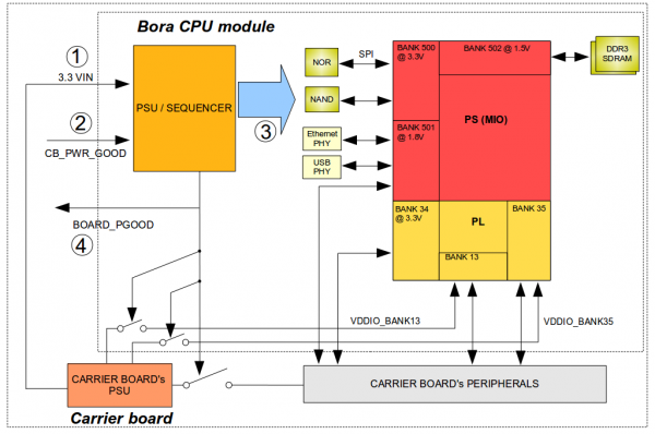
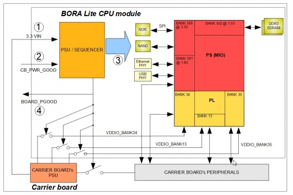
Implementing correct power-up sequence for Zynq-based system is not a trivial task because several power rails are involved. Bora/BORA Lite SOM simplifies this task and embeds all the needed circuitry. The following picture shows a simplified block diagram of power supply subsystem.
The recommended power-up sequence is:
- main power supply rail (3.3VIN) ramps up
- carrier board circuitry raises CB_PWR_GOOD; this indicates 3.3VIN rail is stable (1)
- Bora's PSU enables and sequences DC/DC regulators to turn circuitry on
- BOARD_PGOOD signal is raised; this active-high signal indicates that SoM's I/O is powered. This signal can be used to manage carrier board power up sequence in order to prevent back powering (from SoM to carrier board or vice versa).
Please note that FPGA Bank 13 and FPGA Bank 35 of the PL must be powered by carrier board even if they are not used to implement any function. Two dedicated power rails are available for this purpose (VDDIO_BANK35 and VDDIO_BANK13), offering the system designer the freedom to select the I/O voltage of these two banks. The power rails of both banks are enabled by the BOARD_PGOOD signal and are connected to the I/O power supply rail provided by the carrier board. Bank 13 and bank 35 are High Range (HR), hence the 1.2V - 3.3V voltage range is supported. For more details please refer to [1]. The state of FPGA I/Os prior to configuration is influenced by PUD_C signal as well. For this reason reading of [2] and [3] is also recommended.
Bora's PSU is designed to be robust against misbehaving power rails. However, the recommended power-on ramp for core and I/O supplies ranges from 1 to 6 V/ms.
N.B.: Regarding power off, it is recommended that I/O supply is turned off before core supply.
(1) For BORA SOM this step is not mandatory and CB_PWR_GOOD can be left floating. CB_PWR_GOOD is provided to prevent, if necessary, BORA's PSU to turn on during ramp of carrier board 3.3VIN rail. Depending on carrier board's PSU design, this may lead to undesired glitches during ramp-up.
For BORA Lite SOM, the CB_PWR_GOOD has to be connected to 3.3VIN for always-on operation
XCN15034 and power-off sequence[edit | edit source]
On 29th September 2015 Xilinx released a Product Change Notice indicating new power on/off requirements about Zynq components. A specific analysis has been undertaken with the help of Xilinx technical support to verify the compliance of Bora with respect to the new requirements. This activity has led to the following recommendation: in order to prevent situations that might not fulfill such requirements, 3.3VIN off ramp speed must not exceed 50 V/s.
For more details about this matter, please refer to AR #65240[4] and XCN15034[5].
Reset scheme and voltage monitoring[edit | edit source]
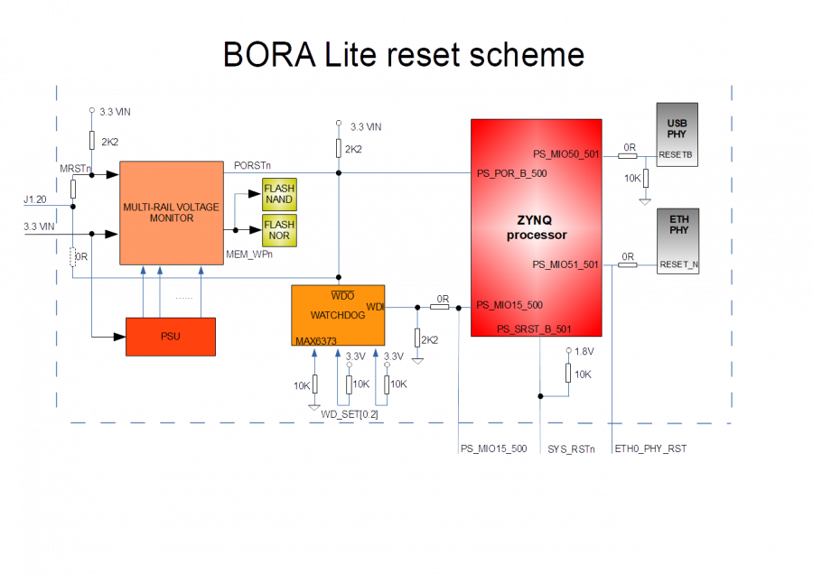
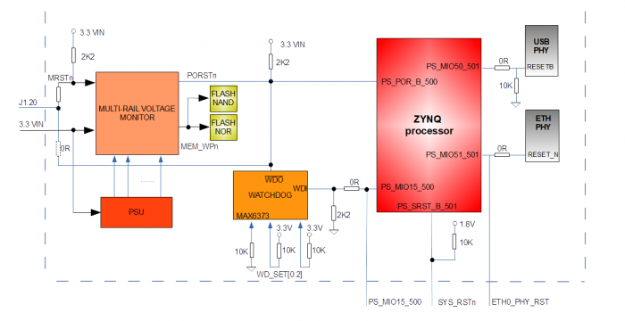
The following picture shows the simplified block diagram of reset scheme and voltage monitoring.
Reset signals[edit | edit source]
The available reset signals are described in detail in the following sections.
MRST[edit | edit source]
MRSTn is a de-bounced input for manual reset (for example to connect a push-button). This signal connected to the voltage monitor and is pulled-up to 3.3VIN through a 2.2kOhm resistor.
PORSTn[edit | edit source]
This is a bidirectonal open-drain signal that is connected to Zynq's PS_POR_B and can be asserted by the following devices:
- a multi-rail voltage monitor that monitors 3.3VIN power rails and all of the rails generated by Bora's PSU. This monitor
- in case of a power glitch, asserts MEM_WPn signal in order to prevent any spurious write operation on flash memories too. MEM_WPn is 3.3V, push-pull, active low.
- has a timeout (set through an on-board capacitor) of about 200 ms.
- provides MRSTn debounced input for manual reset (for example to connect a push-button). This signal is pulled-up to 3.3VIN through a 2.2kOhm resistor.
- a watchdog timer (Maxim MAX6373). For more details please refer to Watchdog section.
PORSTn is pulled-up to 3.3VIN through a 2.2kOhm resistor.
SYS_RSTn[edit | edit source]
This signal is connected to Zynq's PS_SRST_B and is pulled-up to 1.8V through a 10kOhm resistor.
PS_MIO50_501 (USB PHY reset)[edit | edit source]
By default, this signal is connected to the on-board USB PHY reset input as depicted in the above figure. This scheme allows complete software control of the PHY hardware reset regardless of the PL status.
For example, this is how the reset signal is handled in BELK 4.1.5:
- U-Boot
board_initroutine generates a hardware reset pulse. This initializes the component to its default register values. - Linux kernel does not issue any further hardware reset. If a hardware reset is required upon Linux boot up, the
phy-ulpikernel driver and/or the according device tree properties have to be modified for enabling this feature.
PS_MIO51_501 (ETH0 PHY reset)[edit | edit source]
By default, this signal is connected to the on-board Ethernet PHY reset input as depicted in the above figure. This scheme allows complete software control of the PHY hardware reset regardless of the PL status.
For example, this is how the reset signal is handled in BELK 4.1.5:
- U-Boot
board_initroutine generates a hardware reset pulse. This initializes the component to its default register values, which are partly determined by the PHY's strapping pins. - Upon boot up, the Linux kernel issues a software reset via the BCMR register. If a hardware reset is required instead, the
macbkernel driver and/or the related device tree properties have to be modified for enabling this feature.
Pins connection[edit | edit source]
| Pin Name | BORA Lite Pin |
| MRST | J1.20 |
| PORSTn | J1.20 (alternate mount option) |
| SYS_RSTn | J1.18 |
| PS_MIO51_501 | J1.75 |
Clock scheme[edit | edit source]
Bora is equipped with three independent active oscillators:
- processor (33.3 MHz)
- ethernet PHY (25 MHz)
- USB PHY (26 MHz)
Generally speaking, no clocks have to be provided by the carrier board.
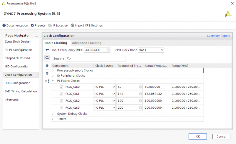
In our Vivado project, the four internal PL fabric clocks have been configured to generate 50, 100, 142 and 200MHz clocks for a general purpose usage: see the processing_system7 section in the Vivado project example bd (block design) file.
System boot[edit | edit source]
The boot process begins at Power On Reset (POR) where the hardware reset logic forces the ARM core to begin execution starting from the on-chip boot ROM. The boot process is multi-stage and minimally includes the Boot ROM and the first-stage boot loader (FSBL). The Zynq-7000 AP SoC includes a factory-programmed Boot ROM that is not useraccessible. The boot ROM:
- determines whether the boot is secure or non-secure
- performs some initialization of the system and cleanups
- reads the mode pins to determine the primary boot device
- once it is satisfied, it executes the FSBL
After a system reset, the system automatically sequences to initialize the system and process the first stage boot loader from the selected external boot device. The process enables the user to configure the AP SoC platform as needed, including the PS and the PL. Optionally, the JTAG interface can be enabled to give the design engineer access to the PS and the PL for test and debug purposes.
Boot options[edit | edit source]
The boot ROM supports configuration from four different slave interfaces:
- Quad-SPI
- NAND
- NOR flash (not available on BORA Lite)
- SD card
Boot mode is selectable via five mode pins (BOOT_MODE[4:0]), and two voltage mode signals, (VMODE[1:0]). The BOOT_MODE pins are MIO[6:2] and the VMODE pins are MIO[8:7]. The pins are used as follows:
| Function | Boot signals | Available options |
|---|---|---|
| JTAG mode | BOOT_MODE[3] MIO[2] |
0: Cascaded JTAG 1: Independent JTAG |
| Boot mode | BOOT_MODE[0-2-1] MIO[5:3] |
000: JTAG 010: NAND 100: Quad-SPI 110: SD card |
| PLLs enable | BOOT_MODE[4] MIO[6] |
0: PLL used 1: PLL bypassed |
| MIO Bank 0 Voltage | VMODE[0] MIO[7] |
0: 2.5 V, 3.3 V 1: 1.8 V |
| MIO Bank 0 Voltage | VMODE[1] MIO[8] |
0: 2.5 V, 3.3 V 1: 1.8 V |
In order to fully understand how boot works on BORA Lite platform, please refer to chapter 6 ("Boot and configuration") of the Zynq7000 Technical Reference Manual.
Default boot configuration[edit | edit source]
Default configuration for BORA Lite module is:
- Mode[0..3] = 1000: Quad-SPI mode
- Mode[4] = 0: PLL not bypassed
- VCFG[0] = 0: 2.5V, 3.3V operations for bank 0
- VCFG[1] = 1: 1.8 operations for bank 1
Assuming that:
- default configuration is not changed
- there's a valid boot code programmed in SPI flash memory the actual boot sequence performed by ARM core will be:
- Bootrom is executed from internal ROM code memory
- FSBL is copied from on-board NOR flash memory connected to SPI0 port to on-chip SRAM by bootrom
- FSBL is executed from on-chip SRAM
- U-Boot bootloader (2nd stage) is copied by FSBL from NOR flash memory connected to Quad-SPI port to SDRAM
- U-boot (2nd stage) is executed from SDRAM
If no boot code is available in SPI NOR flash, the bootrom tries JTAG peripheral booting.
Boot sequence customization[edit | edit source]
BOOT_MODE[4:0] are routed to the J1 connector, enabling for the customization of the boot sequence through a simple resistor network that can be implemented on carrier board hosting BORA Lite module.
| Mode signal | J1 pin | Pin name |
|---|---|---|
| BOOT_MODE[4] | J1.54 | SPI0_SCLK/MODE4/NAND_IO1 |
| BOOT_MODE[3] | J1.46 | SPI0_DQ0/MODE3/NAND_ALE |
| BOOT_MODE[2] | J1.50 | SPI0_DQ2/MODE2/NAND_IO2 |
| BOOT_MODE[1] | J1.48 | SPI0_DQ1/MODE1/NAND_WE |
| BOOT_MODE[0] | J1.52 | SPI0_DQ3/MODE0/NAND_IO0 |
On board JTAG connector[edit | edit source]
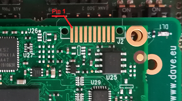
JTAG signals are routed to a dedicated connector (J2) on the BORA Lite PCB. The connector is placed on the top side of the PCB, at the upper-right corner (please see the picture below).
J2 - Connector's pinout[edit | edit source]
J2 footprint mates with Samtec FSI-110-03-G-S connector. The following table reports the connector's pinout:
| Pin# | Pin name | Function | Notes |
|---|---|---|---|
| 1 | DGND | - | - |
| 2 | JTAG_TCK | - | - |
| 3 | JTAG_TMS | - | - |
| 4 | JTAG_TDO | - | - |
| 5 | JTAG_TDI | - | - |
| 6 | FPGA_INIT_B | - | For further details, please refer to PL initialization signals |
| 7 | FPGA_PROGRAM_B | - | For further details, please refer to PL initialization signals
(10 kΩ pull-up resistor is already mounted on BORA module) |
| 8 | FPGA_DONE | - | For further details, please refer to PL initialization signals |
| 9 | D.N.C. | - | RESERVED |
| 10 | 3V3 | - | 3.3VIN enabled with BOARD_PGOOD |
Peripherals[edit | edit source]
Processing System[edit | edit source]
The 54 pins of the MIO module are assigned as reported in the following table:
| MIO Pins | Function |
|---|---|
| MIO[0:14] | Quad-SPI and NAND flash |
| MIO[15] | EX_WDT_REARM (watchdog WDI) Optionally, it can act as SWDT reset out |
| MIO[16:27] | Gigabit Ethernet |
| MIO[28:39] | USB On-The-Go |
| MIO[40:45] | SD/SDIO/MMC |
| MIO[46:47] | I²C0 |
| MIO[48:49] | UART1 |
| MIO[50] | USB PHY reset |
| MIO[51] | ETH0 PHY reset |
| MIO[52] | Ethernet Management Data Clock input |
| MIO[53] | Ethernet Management Data Input/Output |
Programmable logic[edit | edit source]
Introduction[edit | edit source]
The following paragraphs describe in detail the available PL I/O pins and how they are routed to the BORA Lite connector. The Zynq-7000 AP SoC is split into I/O banks to allow for flexibility in the choice of I/O standards, thus each table reports one bank configuration. Moreover, Bora Lite design allows carrier board to power two PL banks in order to achieve complete flexibility in terms of I/O voltage levels too. For more details about PCB design considerations, please refer to the Advanced routing and carrier board design guidelines article.
The following table reports the I/O banks characteristics:
| FPGA Bank | Type | I/O Voltage | Voltage Pins | Notes |
|---|---|---|---|---|
| Bank 13 | High range (HR) | User defined VIO=FPGA_VDDIO_BANK13 1.8 to 3.3V |
J1.41 J1.67 J3.97 J3.98 J3.99 |
Bank 13 is available only with Zynq XC7Z020 part number. Although this bank is not available on Bora SOMs equipped with the XC7Z010 SOC, VDDIO_BANK13 pins must not be left open and must be connected anyway, either to ground or to an external I/O voltage. |
| Bank 34 | High range (HR) | User defined VIO=FPGA_VDDIO_BANK34 1.8 to 3.3V |
J1.77 J1.124 J1.127 J1.129 |
|
| Bank 35 | High range (HR) | User defined VIO=FPGA_VDDIO_BANK35 1.8 to 3.3V |
J1.186 J1.188 J1.192 J1.201 |
Each user I/O is labeled IO_LXXY_Tn_ZZZ_ADi_#, where:
- IO indicates a user I/O pin.
- L indicates a differential pair, with XX a unique pair in the bank and Y = [P|N] for the positive/negative sides of the differential pair.
- Tn indicates the memory byte group [0-3]
- ZZZ indicates a MRCC, SRCC or DQS pin
- ADi indicates a XADC (analog-to-digital converter) differential auxiliary analog input [0–15].
- # indicates the bank number.
Highlighted rows are related to signals that are used for particular functions into the SOM.
FPGA Bank 13 (Zynq 7020 only)[edit | edit source]
N.B. Although BANK 13 is not available on Bora SOMs equipped with the XC7Z010 SOC, VDDIO_BANK13 pins must not be left open and must be connected anyway, either to ground or to an external I/O voltage as described in I/O banks table.
The following table reports the available pins connected to bank 13:
| Pin Name | Conn. Pin | Notes |
| IO_L11P_T1_SRCC_13 | J1.49 | |
| IO_L11N_T1_SRCC_13 | J1.51 | |
| IO_L12P_T1_MRCC_13 | J1.62 | |
| IO_L12N_T1_MRCC_13 | J1.64 | |
| IO_L13N_T2_MRCC_13 | J1.53 | |
| IO_L13P_T2_MRCC_13 | J1.55 | |
| IO_L14N_T2_SRCC_13 | J1.69 | |
| IO_L14P_T2_SRCC_13 | J1.71 | |
| IO_L15N_T2_DQS_13 | J1.59 | |
| IO_L15P_T2_DQS_13 | J1.61 | |
| IO_L16P_T2_13 | J1.63 | |
| IO_L16N_T2_13 | J1.65 | |
| IO_L17N_T2_13 | J1.58 | |
| IO_L17P_T2_13 | J1.60 | |
| IO_L18P_T2_13 | J1.70 | |
| IO_L18N_T2_13 | J1.72 | |
| IO_L19P_T3_13 | J1.66 | |
| IO_L19N_T3_VREF_13 | J1.68 | |
| IO_L20P_T3_13 | J1.78 | |
| IO_L20N_T3_13 | J1.80 | |
| IO_L21N_T3_DQS_13 | J1.74 | |
| IO_L21P_T3_DQS_13 | J1.76 | |
| IO_L22P_T3_13 | J1.45 | |
| IO_L22N_T3_13 | J1.47 | |
| IO_L6N_T0_VREF_13 | J1.43 |
Routing information[edit | edit source]
Routing implemented on Bora SoM allows the use of bank 13's signals as differential pairs as well as single-ended lines. Signals are grouped as denoted by the following table that details routing rules on Bora module. No carrier board guidelines can be provided, because these are application-dependent.
Pairs are highlighted with different colors. When used as differential pairs, differential impedence is 100 Ohm. When used as single-ended signals, impedence is 50 Ohm.
| Bora pin name | Individual net length [mils] |
Intra-pair match [mils] |
Inter-pair match [mils] |
Group Name |
| IO_L11N_T1_SRCC_13 | 963.29 | 5 | 360 | BANK13 Diff group 1 |
| IO_L11P_T1_SRCC_13 | 965.44 | 5 | 360 | BANK13 Diff group 1 |
| IO_L12N_T1_MRCC_13 | 1002.27 | 5 | 360 | BANK13 Diff group 1 |
| IO_L12P_T1_MRCC_13 | 998.73 | 5 | 360 | BANK13 Diff group 1 |
| IO_L13N_T2_MRCC_13 | 819.57 | 5 | 360 | BANK13 Diff group 1 |
| IO_L13P_T2_MRCC_13 | 819.57 | 5 | 360 | BANK13 Diff group 1 |
| IO_L14N_T2_SRCC_13 | 820.26 | 5 | 360 | BANK13 Diff group 1 |
| IO_L14P_T2_SRCC_13 | 821.43 | 5 | 360 | BANK13 Diff group 1 |
| IO_L15N_T2_DQS_13 | 885.06 | 5 | 360 | BANK13 Diff group 1 |
| IO_L15P_T2_DQS_13 | 885.06 | 5 | 360 | BANK13 Diff group 1 |
| IO_L16N_T2_13 | 922.83 | 5 | 360 | BANK13 Diff group 1 |
| IO_L16P_T2_13 | 922.83 | 5 | 360 | BANK13 Diff group 1 |
| IO_L17N_T2_13 | 1007.3 | 5 | 360 | BANK13 Diff group 1 |
| IO_L17P_T2_13 | 1008.75 | 5 | 360 | BANK13 Diff group 1 |
| IO_L18N_T2_13 | 827.46 | 5 | 360 | BANK13 Diff group 1 |
| IO_L18P_T2_13 | 829.35 | 5 | 360 | BANK13 Diff group 1 |
| IO_L19N_T3_VREF_13 | 802.16 | 5 | 360 | BANK13 Diff group 1 |
| IO_L19P_T3_13 | 802.16 | 5 | 360 | BANK13 Diff group 1 |
| IO_L20N_T3_13 | 653.65 | 5 | 360 | BANK13 Diff group 1 |
| IO_L20P_T3_13 | 655.59 | 5 | 360 | BANK13 Diff group 1 |
| IO_L21N_T3_DQS_13 | 738.09 | 5 | 360 | BANK13 Diff group 1 |
| IO_L21P_T3_DQS_13 | 735.9 | 5 | 360 | BANK13 Diff group 1 |
| IO_L22N_T3_13 | 969.5 | 5 | 360 | BANK13 Diff group 1 |
| IO_L22P_T3_13 | 970.21 | 5 | 360 | BANK13 Diff group 1 |
FPGA Bank 34[edit | edit source]
The following table reports the available pins connected to bank 34:
| Pin Name | Conn. Pin | Notes |
| IO_0_34 | J1.79 | |
| IO_25_34 | J1.81 | |
| IO_L1P_T0_34 | J1.84 | |
| IO_L1N_T0_34 | J1.86 | |
| IO_L2P_T0_34 | J1.93 | |
| IO_L2N_T0_34 | J1.95 | |
| IO_L3N_T0_DQS_34 | J1.88 | |
| IO_L3P_T0_DQS_PUDC_B_34 | J1.90 | Internally connected to a 10K pull-up to VDDIO_BANK34 |
| IO_L4P_T0_34 | J1.97 | |
| IO_L4N_T0_34 | J1.99 | |
| IO_L5N_T0_34 | J1.92 | |
| IO_L5P_T0_34 | J1.94 | |
| IO_L6P_T0_34 | J1.110 | |
| IO_L6N_T0_VREF_34 | J1.112 | |
| IO_L7P_T1_34 | J1.89 | |
| IO_L7N_T1_34 | J1.91 | |
| IO_L8N_T1_34 | J1.83 | |
| IO_L8P_T1_34 | J1.85 | |
| IO_L9P_T1_DQS_34 | J1.106 | |
| IO_L9N_T1_DQS_34 | J1.108 | |
| IO_L10P_T1_34 | J1.96 | |
| IO_L10N_T1_34 | J1.98 | |
| IO_L11P_T1_SRCC_34 | J1.105 | |
| IO_L11N_T1_SRCC_34 | J1.107 | |
| IO_L12P_T1_MRCC_34 | J1.130 | Optionally internally connected to RTC/INT_SQW |
| IO_L12N_T1_MRCC_34 | J1.132 | |
| IO_L13N_T2_MRCC_34 | J1.138 | |
| IO_L13P_T2_MRCC_34 | J1.140 | Optionally internally connected to RTC_32KHZ |
| IO_L14P_T2_SRCC_34 | J1.142 | |
| IO_L14N_T2_SRCC_34 | J1.144 | |
| IO_L15P_T2_DQS_34 | J1.118 | |
| IO_L15N_T2_DQS_34 | J1.120 | |
| IO_L16N_T2_34 | J1.115 | |
| IO_L16P_T2_34 | J1.117 | |
| IO_L17P_T2_34 | J1.111 | |
| IO_L17N_T2_34 | J1.113 | |
| IO_L18P_T2_34 | J1.101 | |
| IO_L18N_T2_34 | J1.103 | |
| IO_L19N_T3_VREF_34 | J1.116 | |
| IO_L19P_T3_34 | J1.114 | |
| IO_L20P_T3_34 | J1.134 | |
| IO_L20N_T3_34 | J1.136 | |
| IO_L21P_T3_DQS_34 | J1.102 | |
| IO_L21N_T3_DQS_34 | J1.104 | |
| IO_L22P_T3_34 | J1.126 | |
| IO_L22N_T3_34 | J1.128 | |
| IO_L23N_T3_34 | J1.123 | |
| IO_L23P_T3_34 | J1.125 | |
| IO_L24P_T3_34 | J1.119 | |
| IO_L24N_T3_34 | J1.121 |
Routing information[edit | edit source]
Routing implemented on Bora SoM allows the use of bank 34's signals as differential pairs as well as single-ended lines. Signals are grouped as denoted by the following table that details routing rules on Bora module. No carrier board guidelines can be provided, because these are application-dependent.
Pairs are highlighted with different colors. When used as differential pairs, differential impedence is 100 Ohm. When used as single-ended signals, impedence is 50 Ohm.
| Bora pin name | Individual trace length [mils] |
Intra-pair match [mils] |
Inter-pair match [mils] |
Group name |
| IO_L1N_T0_34 | 821.99 | 5 | 440 | BANK34 Diff group 1 |
| IO_L1P_T0_34 | 821.78 | 5 | 440 | BANK34 Diff group 1 |
| IO_L2N_T0_34 | 679.01 | 5 | 440 | BANK34 Diff group 1 |
| IO_L2P_T0_34 | 684 | 5 | 440 | BANK34 Diff group 1 |
| IO_L3N_T0_DQS_34 | 701.84 | 5 | 440 | BANK34 Diff group 1 |
| IO_L3P_T0_DQS_PUDC_B_34 | 1166.67 | 5 | 440 | BANK34 Diff group 1 |
| IO_L4N_T0_34 | 601.18 | 5 | 440 | BANK34 Diff group 1 |
| IO_L4P_T0_34 | 600.77 | 5 | 440 | BANK34 Diff group 1 |
| IO_L5N_T0_34 | 875.69 | 5 | 440 | BANK34 Diff group 1 |
| IO_L5P_T0_34 | 875.69 | 5 | 440 | BANK34 Diff group 1 |
| IO_L6N_T0_VREF_34 | 863.47 | 5 | 440 | BANK34 Diff group 1 |
| IO_L6P_T0_34 | 866.95 | 5 | 440 | BANK34 Diff group 1 |
| IO_L7N_T1_34 | 727.02 | 5 | 440 | BANK34 Diff group 1 |
| IO_L7P_T1_34 | 727.02 | 5 | 440 | BANK34 Diff group 1 |
| IO_L8N_T1_34 | 800.48 | 5 | 440 | BANK34 Diff group 1 |
| IO_L8P_T1_34 | 798.05 | 5 | 440 | BANK34 Diff group 1 |
| IO_L9N_T1_DQS_34 | 685.07 | 5 | 440 | BANK34 Diff group 1 |
| IO_L9P_T1_DQS_34 | 687.47 | 5 | 440 | BANK34 Diff group 1 |
| IO_L10N_T1_34 | 650.31 | 5 | 440 | BANK34 Diff group 1 |
| IO_L10P_T1_34 | 652.43 | 5 | 440 | BANK34 Diff group 1 |
| IO_L11N_T1_SRCC_34 | 640.93 | 5 | 440 | BANK34 Diff group 1 |
| IO_L11P_T1_SRCC_34 | 636.66 | 5 | 440 | BANK34 Diff group 1 |
| IO_L12N_T1_MRCC_34 | 702.74 | 5 | 440 | BANK34 Diff group 1 |
| IO_L12P_T1_MRCC_34 | 699.86 | 5 | 440 | BANK34 Diff group 1 |
| IO_L13N_T1_MRCC_34 | 844.5 | 5 | 440 | BANK34 Diff group 1 |
| IO_L13P_T1_MRCC_34 | 845.11 | 5 | 440 | BANK34 Diff group 1 |
| IO_L14N_T2_SRCC_34 | 864.85 | 5 | 440 | BANK34 Diff group 1 |
| IO_L14P_T2_SRCC_34 | 862.67 | 5 | 440 | BANK34 Diff group 1 |
| IO_L15N_T2_DQS_34 | 964.59 | 5 | 440 | BANK34 Diff group 1 |
| IO_L15P_T2_DQS_34 | 962.89 | 5 | 440 | BANK34 Diff group 1 |
| IO_L16N_T2_34 | 778.96 | 5 | 440 | BANK34 Diff group 1 |
| IO_L16P_T2_34 | 783.24 | 5 | 440 | BANK34 Diff group 1 |
| IO_L17N_T2_34 | 526.33 | 5 | 440 | BANK34 Diff group 1 |
| IO_L17P_T2_34 | 530.25 | 5 | 440 | BANK34 Diff group 1 |
| IO_L18N_T2_34 | 657.33 | 5 | 440 | BANK34 Diff group 1 |
| IO_L18P_T2_34 | 659.75 | 5 | 440 | BANK34 Diff group 1 |
| IO_L19N_T3_VREF_34 | 723.97 | 5 | 440 | BANK34 Diff group 1 |
| IO_L19P_T3_34 | 727.5 | 5 | 440 | BANK34 Diff group 1 |
| IO_L20N_T3_34 | 728.21 | 5 | 440 | BANK34 Diff group 1 |
| IO_L20P_T3_34 | 728.25 | 5 | 440 | BANK34 Diff group 1 |
| IO_L21N_T3_DQS_34 | 654.43 | 5 | 440 | BANK34 Diff group 1 |
| IO_L21P_T3_DQS_34 | 651.31 | 5 | 440 | BANK34 Diff group 1 |
| IO_L22N_T3_34 | 575.33 | 5 | 440 | BANK34 Diff group 1 |
| IO_L22P_T3_34 | 579.66 | 5 | 440 | BANK34 Diff group 1 |
| IO_L23N_T3_34 | 856.78 | 5 | 440 | BANK34 Diff group 1 |
| IO_L23P_T3_34 | 857.76 | 5 | 440 | BANK34 Diff group 1 |
| IO_L24N_T3_34 | 922.14 | 5 | 440 | BANK34 Diff group 1 |
| IO_L24P_T3_34 | 923.87 | 5 | 440 | BANK34 Diff group 1 |
FPGA Bank 35[edit | edit source]
The following table reports the available pins connected to bank 35:
| Pin Name | Conn. Pin | Notes |
| IO_0_35 | J1.155 | |
| IO_25_35 | J1.157 | |
| IO_L1N_T0_AD0N_35 | J1.193 | |
| IO_L1P_T0_AD0P_35 | J1.195 | |
| IO_L2P_T0_AD8P_35 | J1.197 | |
| IO_L2N_T0_AD8N_35 | J1.199 | |
| IO_L3P_T0_DQS_AD1P_35 | J1.185 | |
| IO_L3N_T0_DQS_AD1N_35 | J1.187 | |
| IO_L4P_T0_35 | J1.182 | |
| IO_L4N_T0_35 | J1.184 | |
| IO_L5P_T0_AD9P_35 | J1.174 | |
| IO_L5N_T0_AD9N_35 | J1.176 | |
| IO_L6N_T0_VREF_35 | J1.177 | |
| IO_L6P_T0_35 | J1.179 | |
| IO_L7P_T1_AD2P_35 | J1.133 | |
| IO_L7N_T1_AD2N_35 | J1.135 | |
| IO_L8N_T1_AD10N_35 | J1.137 | |
| IO_L8P_T1_AD10P_35 | J1.139 | |
| IO_L9P_T1_DQS_AD3P_35 | J1.159 | |
| IO_L9N_T1_DQS_AD3N_35 | J1.161 | |
| IO_L10P_T1_AD11P_35 | J1.145 | |
| IO_L10N_T1_AD11N_35 | J1.147 | |
| IO_L11N_T1_SRCC_35 | J1.141 | |
| IO_L11P_T1_SRCC_35 | J1.143 | |
| IO_L12N_T1_MRCC_35 | J1.171 | |
| IO_L12P_T1_MRCC_35 | J1.173 | |
| IO_L13P_T2_MRCC_35 | J1.189 | |
| IO_L13N_T2_MRCC_35 | J1.191 | |
| IO_L14P_T2_AD4P_SRCC_35 | J1.149 | |
| IO_L14N_T2_AD4N_SRCC_35 | J1.151 | |
| IO_L15N_T2_DQS_AD12N_35 | J1.152 | |
| IO_L15P_T2_DQS_AD12P_35 | J1.154 | |
| IO_L16N_T2_35 | J1.178 | |
| IO_L16P_T2_35 | J1.180 | |
| IO_L17P_T2_AD5P_35 | J1.163 | |
| IO_L17N_T2_AD5N_35 | J1.165 | |
| IO_L18P_T2_AD13P_35 | J1.148 | |
| IO_L18N_T2_AD13N_35 | J1.150 | |
| IO_L19N_T3_VREF_35 | J1.181 | |
| IO_L19P_T3_35 | J1.183 | |
| IO_L20P_T3_AD6P_35 | J1.160 | |
| IO_L20N_T3_AD6N_35 | J1.162 | |
| IO_L21P_T3_DQS_AD14P_35 | J1.167 | |
| IO_L21N_T3_DQS_AD14N_35 | J1.169 | |
| IO_L22N_T3_AD7N_35 | J1.156 | |
| IO_L22P_T3_AD7P_35 | J1.158 | |
| IO_L23N_T3_35 | J1.166 | |
| IO_L23P_T3_35 | J1.168 | |
| IO_L24P_T3_AD15P_35 | J1.170 | |
| IO_L24N_T3_AD15N_35 | J1.172 |
Routing information[edit | edit source]
Routing implemented on Bora SoM allows the use of bank 35's signals as differential pairs as well as single-ended lines. Signals are grouped as denoted by the following table that details routing rules on Bora module. No carrier board guidelines can be provided, because these are application-dependent.
Pairs are highlighted with different colors. When used as differential pairs, differential impedence is 100 Ohm. When used as single-ended signals, impedence is 50 Ohm.
| Bora pin name | Individual trace length [mils] |
Intra-pair match [mils] |
Inter-pair match [mils] |
Group name |
| IO_L1N_T0_AD0N | 1653.52 | 5 | 930 | BANK35 Diff group 1 |
| IO_L1P_T0_AD0P | 1656.04 | 5 | 930 | BANK35 Diff group 1 |
| IO_L2N_T0_AD8N | 1830.25 | 5 | 930 | BANK35 Diff group 1 |
| IO_L2P_T0_AD8P | 1828.16 | 5 | 930 | BANK35 Diff group 1 |
| IO_L3N_T0_DQS_AD1N | 1487.81 | 5 | 930 | BANK35 Diff group 1 |
| IO_L3P_T0_DQS_AD1P | 1487.81 | 5 | 930 | BANK35 Diff group 1 |
| IO_L4N_T0 | 1450.82 | 5 | 930 | BANK35 Diff group 1 |
| IO_L4P_T0 | 1447.23 | 5 | 930 | BANK35 Diff group 1 |
| IO_L5N_T0_AD9N | 1394.95 | 5 | 930 | BANK35 Diff group 1 |
| IO_L5P_T0_AD9P | 1394.98 | 5 | 930 | BANK35 Diff group 1 |
| IO_L6N_T0_VREF | 1501.68 | 5 | 930 | BANK35 Diff group 1 |
| IO_L6P_T0 | 1499.17 | 5 | 930 | BANK35 Diff group 1 |
| IO_L7N_T1_AD2N | 903.67 | 5 | 930 | BANK35 Diff group 1 |
| IO_L7P_T1_AD2P | 900.45 | 5 | 930 | BANK35 Diff group 1 |
| IO_L8N_T1_AD10N | 1106.07 | 5 | 930 | BANK35 Diff group 1 |
| IO_L8P_T1_AD10P | 1106.37 | 5 | 930 | BANK35 Diff group 1 |
| IO_L9N_T1_DQS_AD3N | 1010.9 | 5 | 930 | BANK35 Diff group 1 |
| IO_L9P_T1_DQS_AD3P | 1011.88 | 5 | 930 | BANK35 Diff group 1 |
| IO_L10N_T1_AD11N | 1132.74 | 5 | 930 | BANK35 Diff group 1 |
| IO_L10P_T1_AD11P | 1132.24 | 5 | 930 | BANK35 Diff group 1 |
| IO_L11N_T1_SRCC | 1083.67 | 5 | 930 | BANK35 Diff group 1 |
| IO_L11P_T1_SRCC | 1086.34 | 5 | 930 | BANK35 Diff group 1 |
| IO_L12N_T1_MRCC | 1266.88 | 5 | 930 | BANK35 Diff group 1 |
| IO_L12P_T1_MRCC | 1266.88 | 5 | 930 | BANK35 Diff group 1 |
| IO_L13N_T2_MRCC | 1561.25 | 5 | 930 | BANK35 Diff group 1 |
| IO_L13P_T2_MRCC | 1565.9 | 5 | 930 | BANK35 Diff group 1 |
| IO_L14N_T2_AD4N_SRCC | 1310.96 | 5 | 930 | BANK35 Diff group 1 |
| IO_L14P_T2_AD4P_SRCC | 1314.72 | 5 | 930 | BANK35 Diff group 1 |
| IO_L15N_T2_DQS_AD12N | 1390.3 | 5 | 930 | BANK35 Diff group 1 |
| IO_L15P_T2_DQS_AD12P | 1390.3 | 5 | 930 | BANK35 Diff group 1 |
| IO_L16N_T2 | 1328.03 | 5 | 930 | BANK35 Diff group 1 |
| IO_L16P_T2 | 1323.99 | 5 | 930 | BANK35 Diff group 1 |
| IO_L17N_T2_AD5N | 1066.44 | 5 | 930 | BANK35 Diff group 1 |
| IO_L17P_T2_AD5P | 1066.44 | 5 | 930 | BANK35 Diff group 1 |
| IO_L18N_T2_AD13N | 1274.72 | 5 | 930 | BANK35 Diff group 1 |
| IO_L18P_T2_AD13P | 1271.59 | 5 | 930 | BANK35 Diff group 1 |
| IO_L19N_T3_VREF | 1491.93 | 5 | 930 | BANK35 Diff group 1 |
| IO_L19P_T3 | 1490.98 | 5 | 930 | BANK35 Diff group 1 |
| IO_L20N_T3_AD6N | 1348.54 | 5 | 930 | BANK35 Diff group 1 |
| IO_L20P_T3_AD6P | 1348.54 | 5 | 930 | BANK35 Diff group 1 |
| IO_L21N_T3_DQS_AD14N | 1217.94 | 5 | 930 | BANK35 Diff group 1 |
| IO_L21P_T3_DQS_AD14P | 1219.83 | 5 | 930 | BANK35 Diff group 1 |
| IO_L22N_T3_AD7N | 1209.1 | 5 | 930 | BANK35 Diff group 1 |
| IO_L22P_T3_AD7P | 1212.95 | 5 | 930 | BANK35 Diff group 1 |
| IO_L23N_T3 | 1279.78 | 5 | 930 | BANK35 Diff group 1 |
| IO_L23P_T3 | 1282 | 5 | 930 | BANK35 Diff group 1 |
| IO_L24N_T3_AD15N | 1282.1 | 5 | 930 | BANK35 Diff group 1 |
| IO_L24P_T3_AD15P | 1279.15 | 5 | 930 | BANK35 Diff group 1 |
Gigabit Ethernet[edit | edit source]
On-board Ethernet PHY (Micrel KSZ9031RNX) provides interface signals required to implement the 10/100/1000 Mbps Ethernet port. The transceiver is connected to the Gigabit Ethernet Controller (GEM) through RGMII interface on MIO bank 1, pins PS_MIO[16:27]. For further details (eg: connection and selection of the magnetics), please refer to the Micrel KSZ9031RNX datasheet. The following table describes the interface signals:
| Pin name | Conn. pin | Function | Notes |
|---|---|---|---|
| ETH_TXRX0_P | J1.19 | Media Dependent Interface[0], positive pin | - |
| ETH_TXRX0_M | J1.21 | Media Dependent Interface[0], negative pin | - |
| ETH_TXRX1_P | J1.23 | Media Dependent Interface[1], positive pin | - |
| ETH_TXRX1_M | J1.25 | Media Dependent Interface[1], negative pin | - |
| ETH_TXRX2_P | J1.27 | Media Dependent Interface[2], positive pin | - |
| ETH_TXRX2_M | J1.29 | Media Dependent Interface[2], negative pin | - |
| ETH_TXRX3_P | J1.31 | Media Dependent Interface[3], positive pin | - |
| ETH_TXRX3_M | J1.33 | Media Dependent Interface[3], negative pin | - |
| ETH_LED1 | J1.13 | Activity LED | - |
| ETH_LED2 | J1.15 | Link LED | - |
USB[edit | edit source]
BORA Lite provides one USB 2.0 (Full Speed, up to 480 Mbps) port with on-board PHY (SMSC USB3317) and support to the On-The-Go (OTG) specifications. The transceiver is connected to the USB1 controller (MIO bank 1, pins PS_MIO[28:39]). The following table describes the interface signals:
| Pin name | Conn. pin | Function | Notes |
|---|---|---|---|
| USBP1 | J1.200 | D+ pin of the USB cable | - |
| USBM1 | J1.202 | D- pin of the USB cable | - |
| USBOTG_CPEN | J1.194 | External 5 volt supply enable | This pin is used to enable the external Vbus power supply |
| OTG_VBUS | J1.196 | VBUS pin of the USB cable | - |
| OTG_ID | J1.198 | ID pin of the USB cable | For non-OTG applications this pin can be floated. For an A-device ID is grounded. For a B-device ID is floated. |
SD/SDIO[edit | edit source]
The SD/SDIO controller controller is compatible with the standard SD Host Controller Specification Version 2.0 Part A2. The core also supports up to seven functions in SD1, SD4, but does not support SPI mode. It does support SD high-speed (SDHS) and SD High Capacity (SDHC) card standards. The SD/SDIO controller also supports MMC3.31.
The following table describes the interface signals:
| Pin name | Conn. pin | Function | Notes |
|---|---|---|---|
| PS_SD0_CLOCK | J1.37 | SD/SDIO/MMC clock | - |
| PS_SD0_CMD | J1.39 | SD/SDIO/MMC command | - |
| PS_SD0_DAT0 | J1.40 | SD/SDIO/MMC data 0 | - |
| PS_SD0_DAT1 | J1.38 | SD/SDIO/MMC data 1 | - |
| PS_SD0_DAT2 | J1.36 | SD/SDIO/MMC data 2 | - |
| PS_SD0_DAT3 | J1.34 | SD/SDIO/MMC data 3 | - |
QUAD SPI[edit | edit source]
Quad-SPI is used to access multi-bit serial flash memory devices for high throughput and low pin count applications. The controller operates in one of three modes: I/O mode, linear addressing mode, and legacy SPI mode. The following table describes the interface signals:
| Pin name | Conn. pin | Function | Notes |
|---|---|---|---|
| SPI0_CS0 | J1.44 | Chip select 0 | MIO bank 0, pin 1 |
| SPI0_DQ0 | J1.46 | 1-bit: Master Output 2-bit: I/O0 4-bit: I/O0 |
MIO bank 0, pin 2 |
| SPI0_DQ1 | J1.48 | 1-bit: Master Input 2-bit: I/O1 4-bit: I/O1 |
MIO bank 0, pin 3 |
| SPI0_DQ2 | J1.50 | 1-bit: Write protect 2-bit: Write protect 4-bit: I/O0 |
MIO bank 0, pin 4 |
| SPI0_DQ3 | J1.52 | 1-bit: Hold 2-bit: Hold 4-bit: I/O3 |
MIO bank 0, pin 5 |
| SPI0_SCLK | J1.54 | Serial clock | MIO bank 0, pin 6 |
Static memory controller (NAND)[edit | edit source]
Static memory controller (SMC) signals are routed to the connectors to connect an external flash NAND memory chip. The following table describes the interface signals:
| Pin name | Conn. pin | Function | Notes |
|---|---|---|---|
| NAND_CS0 | J1.122 | NAND flash chip select | MIO bank 0, pin 0 |
| NAND_IO0 | J1.119 | NAND I/O 0 | MIO bank 0, pin 5 |
| NAND_IO1 | J1.129 | NAND I/O 1 | MIO bank 0, pin 6 |
| NAND_IO2 | J1.121 | NAND I/O 2 | MIO bank 0, pin 4 |
| NAND_IO3 | J1.124 | NAND I/O 3 | MIO bank 0, pin 13 |
| NAND_IO4 | J1.126 | NAND I/O 4 | MIO bank 0, pin 9 |
| NAND_IO5 | J1.128 | NAND I/O 5 | MIO bank 0, pin 10 |
| NAND_IO6 | J1.132 | NAND I/O 6 | MIO bank 0, pin 11 |
| NAND_IO7 | J1.134 | NAND I/O 7 | MIO bank 0, pin 12 |
| NAND_WE | J1.123 | NAND write enable | MIO bank 0, pin 3 |
| NAND_ALE | J1.125 | NAND address latch | MIO bank 0, pin 2 |
| NAND_BUSY | J1.131 | NAND Busy | MIO bank 0, pin 14 |
| NAND_RE | J1.136 | NAND read enable | MIO bank 0, pin 8 |
| NAND_CLE | J1.138 | NAND command latch enable | MIO bank 0, pin 7 |
I^2C0[edit | edit source]
This I²C module is a bus controller that can function as a master or a slave in a multi-master design. It supports an extremely wide clock frequency range up to 400 Kb/s. I²C0 is internally connected to the following devices:
The following table describes the interface signals:
| Pin name | Conn. pin | Function | Notes |
|---|---|---|---|
| PS_MIO46_501 | J1.32 | I2C clock | - |
| PS_MIO47_501 | J1.28 | I2C data | - |
UART 1[edit | edit source]
The UART controller is a full-duplex asynchronous receiver and transmitter that supports a wide range of programmable baud rates and I/O signal formats. UART1 port is routed to the SOM connectors as a 2-wire interface. The following table describes the interface signals:
| Pin name | Conn. pin | Function | Notes |
|---|---|---|---|
| PS_UART1_RX | J1.24 | UART Receive line | - |
| PS_UART1_TX | J1.26 | UART Transmit line | - |
JTAG[edit | edit source]
The Zynq-7000 family of AP SoC devices provides debug access via a standard JTAG (IEEE 1149.1) debug interface. This JTAG port grants access to the device chain composed of both the CPU core and the FPGA part. The following table describes the interface signals:
| Pin name | Conn. pin | Function | Notes |
|---|---|---|---|
| JTAG_TCK | J2.2 | JTAG TCK | - |
| JTAG_TMS | J2.3 | JTAG TMS | - |
| JTAG_TDO | J2.4 | JTAG TDO | - |
| JTAG_TDI | J2.5 | JTAG TDI | - |
More information about the JTAG connector at the this page
EEPROM[edit | edit source]
An on-board Microchip 24AA32AT device provides an added storage device for factory settings:
- the first 32 bytes of the device are RESERVED: this region stores the bytes for the ConfigID on BORA Lite SOMs configured for booting from NAND device (without NOR SPI on board)
- the device is write protected using the EEPROM_WP
The device has some configuration pins:
- three address pins for configuring the I2C adddress A0, A1, A2 internally configured as A[0..2]='000'
- the EEPROM_WP is connected to J2.9 pin on the JTAG connector and should not be externally connected
Real Time Clock[edit | edit source]
An on-board Maxim Integrated DS3232 device provides a very accurate, temperature-compensated real-time clock (RTC) resource with:
- Temperature-compensated crystal oscillator
- Date, time and calendar
- Alarm capability
- Backup power from external battery
- ±3.5ppm accuracy from -40°C to +85°C
- 236 Bytes of Battery-Backed SRAM
- I²C Interface
Backup power is provided through the RTC_VBAT signal connected to J1.22
If not used, RTC_VBAT must be externally connected to GND. For a detailed description of RTC characteristics, please refer to the DS3232 datasheet.
Watchdog[edit | edit source]
An external watchdog timer (WDT), Maxim MAX6373[6]), is connected to the PORSTn signal. During normal operation, the microprocessor should repeatedly toggle the watchdog input WDI before the selected watchdog timeout period elapses to demonstrate that the system is processing code properly. If the µP does not provide a valid watchdog input transition before the timeout period expires, the supervisor asserts a watchdog (WDO) output to signal that the system is not executing the desired instructions within the expected time frame. The watchdog output pulse is used to reset the µP.
The default mounting option is depicted in the following figure.
WDI is connected to Zynq's PS_MIO15_500 I/O. This signal is available on Bora connectors as PS_MIO15_500 (J1.42).
MAX6373 timeout is pin-selectable. It can be configured through the WD_SET0, WD_SET1 and WD_SET2 signals. The pins are configured internally to the BORA Lite SOM, by default, as follows:
- WD_SET2 = 1
- WD_SET1 = 1
- WD_SET0 = 0
This set selects the option (the exhaustive list of configurations options is described in table 1 of reference [6]):
- tDELAY = first edge
- tWD = 10s.
In other words, WDT is started when the first transition on WDI input is detected. Once started, its timeout period is 10s. A 2.2kOhm pull-down is internally connected to the PS_MIO15_500 signal in order to avoid WDT may be inadvertently started at power-up. In general, the first transition of WDI input should be under software control (connected to PS_MIO15_500 GPIO pad) .
In any case, when the watchdog is started, the software (bootloader/operating system) must take care of toggling the watchdog trigger pin (WDI) before the timeout expiration.
Selecting different configurations[edit | edit source]
Since WD_SETx signals are routed internally, WDT configuration can be changed by ordering a Custom BORA Lite configuration: please contact our Sales department for a Custom BORA Lite order code.
It is also worth mentioning that Zynq integrates a System Watchdog Timer (SWDT) that can optionally generate a reset pulse on PS_MIO15_500 pad if this is configured as SWDT reset. In case such a configuration is of interest, on request, MAX6373 may not be populated. For more details about this option, please contact Sales Department.
References[edit | edit source]
Electrical, Thermal and Mechanical Features[edit | edit source]
Operational characteristics[edit | edit source]
Maximum ratings[edit | edit source]
| Parameter | Min | Typ | Max | Unit |
|---|---|---|---|---|
| Main power supply voltage | -0.3 | 3.3 | 3.6 | V |
Recommended ratings[edit | edit source]
| Parameter | Min | Typ | Max | Unit |
|---|---|---|---|---|
| Main power supply voltage | 3.135 | 3.3 | 3.465 | V |
Power consumption[edit | edit source]
Providing theoretical maximum power consumption value would be useless for the majority of system designers building their application upon BORA Lite module. Practically speaking, these figures would be of no help when it comes to size power supply unit or to perform thermal design of real systems.
Instead, several configurations have been tested in order to provide figures that are measured on real-world use cases.
Please note that BORA Lite platform is so flexible that it is virtually impossible to test for all possible configurations and applications on the market. The use cases here presented should cover most of real-world scenarios. However actual customer's application might require more power than values reported here or customer's use case may be differ significantly with respect to the ones here considered.
Therefore, application-specific requirements have always to be taken into consideration in order to size power supply unit and to implement thermal management properly.
Use cases results[edit | edit source]
Measurements have been performed on the BORA Lite SOM under test is equipped with:
- XC7Z020-1
- 1 GB DDR3L SDRAM
- 16 MB NOR SPI
- 1 GB NAND SLC
Test conditions[edit | edit source]
- 2 x burnCortexA9
- FPGA test bitstream
- memtester 50M loop
- file copy and verify (md5sum) on SD card
- file copy and verify (md5sum) on USB memory key
- mtd test on NAND
- mtd_speedtest
- mtd_stresstest
- mtd_readtest
- mtd_pagetest
- mtd_subpagetest
- iperf (client) loop on eth0
The table below reports the power consumption measurements for the considered use cases.
| Test type | Power (mW) |
|---|---|
| Stress test | max 7.85W (mean 3.37 W) |
Electrical Thermal management and heat dissipation[edit | edit source]
Providing maximum power consumption of a system-on-module (SOM for short) is virtually impossible because it is extremely hard to define the worst case. This is even more true in case of BORA Lite , where this is affected by the software running on Processing System (PS) side and the Programmable Logic (PL) configuration.
For this reason, several real use cases have been considered rather than indicating a theoretical maximum power consumption value that would be useless for the majority of system integrators, because it likely would lead to an oversized power supply unit.
Again, it is worth remembering that BORA Lite platform is so flexible that is practically impossible to test for all possible configurations and applications on the market. The use cases here presented should cover most of the real-world scenarios. However, actual customer applications might require more power than the values reported here. Generally speaking, application-specific requirements have to be taken into consideration in order to size the power supply unit and to implement thermal management properly.
The following sections describe in detail the testbeds that have been used. All of them make use of a specific FPGA bistream that has been developed to perform stress tests on BORA Lite platforms [1]. These tests have been conducted in a climatic chamber that allows setting environment temperature surrounding DUT, denoted in the rest of the document as Tamb. Tj denotes Zynq's junction temperature instead.
FPGA bitstream - that in turn is built upon this core - allocates most of FPGA resources. All of them are clocked by one clock signal whose frequency is selectable by the PS at runtime. This allows to flexibly change DUT current absorption and, consequently, the heat it generates.
For information related to temperature measurements, see also this section.
[1] These tests are part of the standard qualification procedure of DAVE Embedded Systems products. Their primary goal is to verify the proper operating of the DUT under conditions of usage that are extremely demanding. Data reported here were excerpted from the logs generated by such tests.
Configuration[edit | edit source]
Testbed[edit | edit source]
Measurements have been performed on the following platform:
- BORA Lite SOM: DBTD4111I0R
- this model is based on Zynq XC7Z020-1I (Tj: -40°C / +100°C)
- carrier board: BORAX EVB
- processor frequency: 667 MHz
- FPGA frequency
- 1 MHz (Tamb = +85°C)
- 140 MHz (Tamb = +-40°C)
- U-Boot:
2017.01-belk-4.1.4 (Jul 28 2021 - 23:20:09 +0200), Build: belk-4.1.4 - Linux kernel:
4.9.0-belk-4.1.0-xilinx (jenkins@linuxserver2) (gcc version 6.2.1 20161016 (Linaro GCC 6.2-2016.11) ) #1 SMP PREEMPT Tue Dec 24 11:34:28 CET 2019 - root file system mounted over Gigabit Ethernet link.
Please note that, when Tamb has been set to +85°C, the BORA LiteSOM has been coupled to a passive heat sink to prevent exceeding maximum Zynq's junction temperature.
At the application level, PS executes concurrently several tasks including:
- two instances of
burnCortexA9 - periodic reading of Zynq's ADCs
- periodic reading of voltage/current probe (Texas Instruments INA226) connected to the SOM's power rail
- one instance of
memtester, exercising 50 MByte of SDRAM - endless loop of writing/reading/verifying operations on microSD card
- endless loop of writing/reading/verifying operations on memory stick connected to the USB port
- mtd_test on NAND (mtd_speedtest, mtd_stresstest, mtd_readtest, mtd_pagetest, mtd_subpagetest)
- ethernet iperf
Results[edit | edit source]
- Tamb: temperature of the ambient surrounding the DUT
- Tj_max: maximum Zynq's junction temperature measured during the test
- P_max: maximum power absorption of BORA Lite SOM
| Tamb [°C] | Tj_max [°C] | FPGA clock frequency [MHz] | P_max [W] |
|---|---|---|---|
| 85 | 116.4 [1] | 1 | 7.85 |
| -40 | 56.8 | 140 | 7.87 |
[1] In spite of the use of heat sink, this value exceeds maximum valued declared by the manufacturer. This is acceptable in case of stress tests, where it is possible that parts of the DUT get damaged.
Hotspots[edit | edit source]
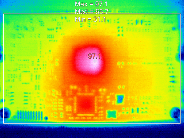
The following picture illustrates the two typical hotsposts when the BORA Lite SOM is running: as seen in the picture, the SOC and the ethernet PHY are the two hottest points to take into account for the Power dissipation management
Mechanical specifications[edit | edit source]
This chapter describes the mechanical characteristics of the BORA Lite module.
Board Layout[edit | edit source]
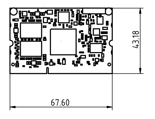
The following figure shows the physical dimensions (expressed in mm) of the BORA Lite module:
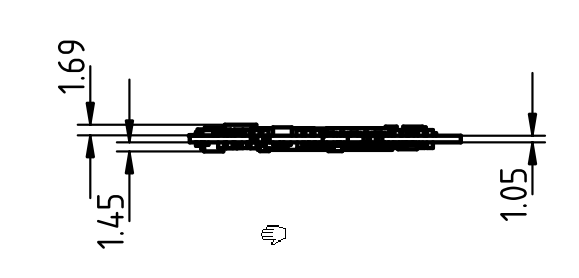
The following figure highlights the maximum components' heights (expressed in mm) on BORA Lite module:
Connector[edit | edit source]
The following figure shows the BORA Lite connector layout:
CAD drawings[edit | edit source]
- DXF (2D): boraLite.dxf.zip
- STEP (3D): boraLite_stp.zip
3D drawings[edit | edit source]
- ↑ Xilinx, DS187 Zynq-7000 All Programmable SoC (Z-7010, Z-7015, and Z-7020): DC and AC Switching Characteristics
- ↑ http://www.xilinx.com/support/answers/45985.html
- ↑ http://www.xilinx.com/support/answers/50802.html
- ↑ http://www.xilinx.com/support/answers/65240.html
- ↑ http://www.xilinx.com/support/documentation/customer_notices/xcn15034.pdf
- ↑ 6.0 6.1 https://www.maximintegrated.com/en/products/power/supervisors-voltage-monitors-sequencers/MAX6373.html
