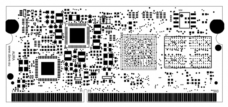
AURA SOM/AURA Hardware/pdf
General Information[edit | edit source]
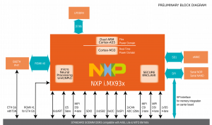
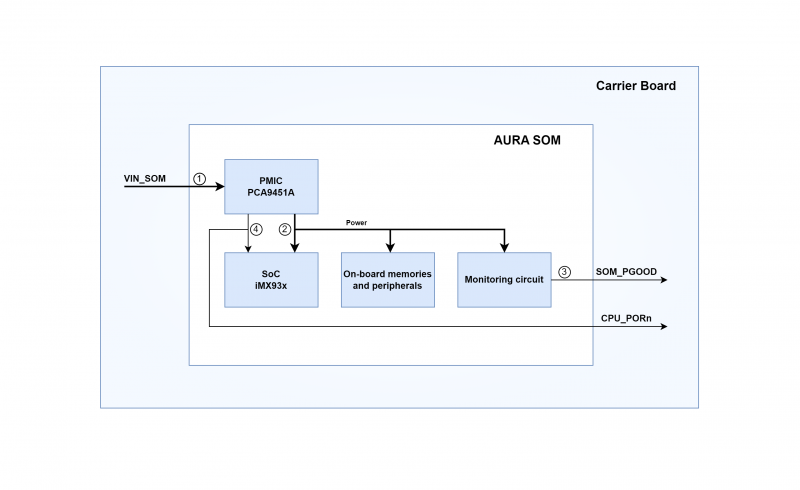
AURA Block Diagram[edit | edit source]
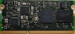
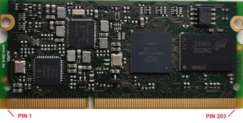
AURA TOP View[edit | edit source]
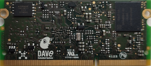
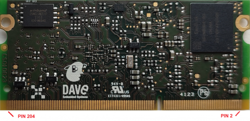
AURA BOTTOM View[edit | edit source]
Processor and memory subsystem[edit | edit source]
The heart of AURA module is composed by the following components:
- i.MX93 SoC application processor
- Power supply unit
- LPDDR4 memory bank
- eMMC or NAND flash banks
- Connectors:
- 1 x 204 pins SO-DIMM edge connector with interfaces signals partially compatible with AXEL Lite SOM
This chapter shortly describes the main AURA components.
Processor Info[edit | edit source]
| Processor | i.MX933x | i.MX935x | |
| # Cores | 1x or 2x Arm® Cortex®-A55
1x Arm® Cortex®-M33 |
1x or 2x Arm® Cortex®-A55
1x Arm® Cortex®-M33 1x NPU | |
| Clock | 1.7 GHz (Industrial) | ||
| L3
Cache |
256 KB | ||
| LPDDR4 | 32 bit @ 1600 MHz with inline ECC
(LPDDR4-3200) | ||
| Video | PXP 2D accelerator | ||
| NPU | 0.5 TOPs Neural Processing Unit | ||
| Display
Controller |
LVDS channel
up to 1366x768 or 1280x800 | ||
| Video
Output |
1x 4-lane MIPI-DSI | ||
| Camera
Input |
1x MIPI CSI | ||
| Ethernet | 2x 1Gbit ethernet | ||
| USB | 2x USB 2.0 OTG | ||
RAM memory bank[edit | edit source]
LPDD4 SDRAM memory bank is composed by 1x 16-bit width chip. The following table reports the SDRAM specifications:
| CPU connection | Multi-mode DDR controller (MMDC) |
| Size max | 2 GB |
| Width | 16 bit |
| Speed | 1400 MHz |
eMMC flash bank[edit | edit source]
On board main storage memory eMMC is connected to the SDIO1 interface and it can act as boot peripheral. The following table reports the eMMC flash specifications:
| CPU connection | SDIO1 |
| Size min | 4 GB |
| Size max | 64 GB |
| Bootable | Yes |
NAND flash bank[edit | edit source]
Alternative option for main storage memory can be a serial NAND flash connected to the CPU's Quad serial flash controller. It can act as boot peripheral. The following table reports the NAND flash specifications:
| CPU connection | SPI Serial NAND flash controller |
| Size min | 16GB |
| Size max | 128GB |
| Width | 1,4,8 bit mode |
| Bootable | Yes |
Memory map[edit | edit source]
For detailed information, please refer to chapter 2 “Memory Maps” of the i.MX93 Applications Processor Reference Manual
Power supply unit[edit | edit source]
AURA embeds all the elements required for powering the unit, therefore power sequencing is self-contained and simplified. Nevertheless, power must be provided from carrier board, and therefore users should be aware of the ranges power supply can assume as well as all other parameters.
Hardware versioning and tracking[edit | edit source]
AURA SOM implements well established versioning and tracking mechanisms:
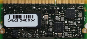
- PCB version is copper printed on PCB itself, as shown in Fig. 1
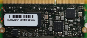
- serial number: it is printed on a white label, as shown in Fig. 2: see also Product serial number page for more details
- ConfigID: it is used by software running on the board for the identification of the product model/hardware configuration. For more details, please refer to this link
- On AURA SOM ConfigID is stored in these areas of OTP
Part number composition[edit | edit source]
AURA SOM module part number is composed by several fields as follows.
[Family][SOC][RAM][Storage][Boot Mode][RFU][RFU][Temperature range][PCB revision][Manufacturing option][Software Configuration]
Each field is detailed in the following table.
| Part number structure | Options | Description | |||||||||||||||||||||||||||||||||||||||||||||||||||||||||||||||||||||||||||||||||||||
|---|---|---|---|---|---|---|---|---|---|---|---|---|---|---|---|---|---|---|---|---|---|---|---|---|---|---|---|---|---|---|---|---|---|---|---|---|---|---|---|---|---|---|---|---|---|---|---|---|---|---|---|---|---|---|---|---|---|---|---|---|---|---|---|---|---|---|---|---|---|---|---|---|---|---|---|---|---|---|---|---|---|---|---|---|---|---|---|
| Family | DAU | Family prefix code | |||||||||||||||||||||||||||||||||||||||||||||||||||||||||||||||||||||||||||||||||||||
| SOC |
|
These options depends on NXP P/N description available here. Other versions can be available, please contact technical support | |||||||||||||||||||||||||||||||||||||||||||||||||||||||||||||||||||||||||||||||||||||
| RAM |
|
||||||||||||||||||||||||||||||||||||||||||||||||||||||||||||||||||||||||||||||||||||||
| Storage
eMMC/NAND/QSPI |
|
SPI NOR and NAND are alternatives mounting options | |||||||||||||||||||||||||||||||||||||||||||||||||||||||||||||||||||||||||||||||||||||
| Boot Mode: |
|
The boot modes listed here are "single boot", meaning that the Cortex-A55 is the first core to boot.
Other options are available on-demand, however. DAVE Embedded Systems' team is available for additional information on this matter. If necessary, please contact sales@dave.eu. | |||||||||||||||||||||||||||||||||||||||||||||||||||||||||||||||||||||||||||||||||||||
| RFU |
|
||||||||||||||||||||||||||||||||||||||||||||||||||||||||||||||||||||||||||||||||||||||
| RFU |
|
||||||||||||||||||||||||||||||||||||||||||||||||||||||||||||||||||||||||||||||||||||||
| Temperature range |
|
||||||||||||||||||||||||||||||||||||||||||||||||||||||||||||||||||||||||||||||||||||||
| PCB revision |
|
PCB release may change for manufacturing purposes (i.e. text fixture adaptation) | |||||||||||||||||||||||||||||||||||||||||||||||||||||||||||||||||||||||||||||||||||||
| Manufacturing option |
|
typically connected to production process and quality | |||||||||||||||||||||||||||||||||||||||||||||||||||||||||||||||||||||||||||||||||||||
| Software Configuration |
|
If customers require custom SW deployed this section should be defined and agreed. Please contact technical support |
Example[edit | edit source]
AURA SOM code DAUB13100I0R-00
- B: MIMX9352DVVxMAB 1.7GHz Dual Core Tj: (0+95) Full Feature
- 1: 1GB LPDDR4
- 3: 8GB eMMC
- 1: eMMC boot
- 0: RFU
- 0: RFU
- I: Industrial grade: -40 to +85°C
- 0: first version
- R: RoHS compliant
- -00: standard factory u-boot pre-programmed
Pinout Table[edit | edit source]
Connectors and Pinout Table[edit | edit source]
Connectors description[edit | edit source]
In the following table are described all available connectors integrated on AURA SOM:
| Connector name | Connector Type | Notes | Carrier board counterpart |
|---|---|---|---|
| J1 | SODIMM DDR3 edge connector 204 pin | TE Connectivity 2013289-1 |
The dedicated carrier board must mount the mating connector and connect the desired peripheral interfaces according to AURA pinout specifications. See the images below for reference:
Pinout table naming conventions[edit | edit source]
This chapter contains the pinout description of the AURA module, grouped in two tables (odd and even pins) that report the pin mapping of the 204-pin SO-DIMM AURA connector.
Each row in the pinout tables contains the following information:
| Pin | Reference to the connector pin |
| Pin Name | Pin (signal) name on the AURA connectors |
| Internal connections |
Connections to the AURA components
|
| Ball/pin # | Component ball/pin number connected to signal |
| Voltage | I/O voltage levels |
| Type | Pin type:
|
| Notes | Remarks on special pin characteristics |
| Pin MUX alternative functions | Muxes:
The number of functions depends on platform |
Voltage domains[edit | edit source]
| Voltage domain | Nominal voltage [V] | Notes |
|---|---|---|
| 3.3VIN | 3.3 | See Operational_characteristics of the SoM wiki page |
| NVCC_3V3 | 3.3 | Voltage generated by the internal PSU. See Power Supply Unit (PSU) wiki page |
| VDD_ANA_1V8 | 1.8 |
Pinout table XLS file[edit | edit source]
For your convenience, please find a spreadsheet with the AURA/MIMX935x pinout and pinmux table here.
Pinout Table ODD pins declaration[edit | edit source]
| Pin | Pin Name | Internal Connections | Ball/pin # | Voltage
domain |
Type | Notes | Alternative Functions | |
|---|---|---|---|---|---|---|---|---|
| J1.1 | DGND | DGND | - | - | G | |||
| J1.3 | 3.3VIN | INPUT VOLTAGE | - | 3.3VIN | S | |||
| J1.5 | 3.3VIN | INPUT VOLTAGE | - | 3.3VIN | S | |||
| J1.7 | 3.3VIN | INPUT VOLTAGE | - | 3.3VIN | S | |||
| J1.9 | 3.3VIN | INPUT VOLTAGE | - | 3.3VIN | S | |||
| J1.11 | DGND | DGND | - | - | G | |||
| J1.13 | ETH1_LED1 | LAN.LED1/GPIO0 | 18 | NVCC_3V3 | O | |||
| J1.15 | ETH1_LED2 | LAN.LED2/GPIO1 | 16 | NVCC_3V3 | O | |||
| J1.17 | DGND | DGND | - | - | G | |||
| J1.19 | ETH1_TXRX0_P | LAN.TXRXP_A | 2 | NVCC_3V3 | D | |||
| J1.21 | ETH1_TXRX0_M | LAN.TXRXM_A | 3 | NVCC_3V3 | D | |||
| J1.23 | ETH1_TXRX1_P | LAN.TXRXP_B | 5 | NVCC_3V3 | D | |||
| J1.25 | ETH1_TXRX1_M | LAN.TXRXM_B | 6 | NVCC_3V3 | D | |||
| J1.27 | ETH1_TXRX2_P | LAN.TXRXP_C | 7 | NVCC_3V3 | D | |||
| J1.29 | ETH1_TXRX2_M | LAN.TXRXM_C | 8 | NVCC_3V3 | D | |||
| J1.31 | ETH1_TXRX3_P | LAN.TXRXP_D | 10 | NVCC_3V3 | D | |||
| J1.33 | ETH1_TXRX3_M | LAN.TXRXM_D | 11 | NVCC_3V3 | D | |||
| J1.35 | DGND | DGND | - | - | G | |||
| J1.37 | ETH1_LED3 | LAN.LED3/GPIO2 | 15 | NVCC_3V3 | O | |||
| J1.39 | ETH1_LED4 | LAN.LED4/GPIO3 | 14 | NVCC_3V3 | O | |||
| J1.41 | ETH_OSC_EN | 46 | NVCC_3V3 | I | Hardware mounting option | |||
| J1.43 | GPIO_IO06 | CPU.GPIO_IO06 | L20 | NVCC_3V3 | IO | Pin ALT-0 | GPIO2_IO06 | |
| Pin ALT-1 | TPM5_CH0 | |||||||
| Pin ALT-2 | PDM_BIT_STREAM01 | |||||||
| Pin ALT-3 | DISP_DATA02 | |||||||
| Pin ALT-4 | SPI7_SOUT | |||||||
| Pin ALT-5 | UART6_CTS_B | |||||||
| Pin ALT-6 | I2C7_SDA | |||||||
| Pin ALT-7 | FLEXIO1_FLEXIO06 | |||||||
| J1.45 | GPIO_IO18 | CPU.GPIO_IO18 | R18 | NVCC_3V3 | IO | Pin ALT-0 | GPIO2_IO18 | |
| Pin ALT-1 | SAI3_RX_BCLK | |||||||
| Pin ALT-2 | CAM_DATA09 | |||||||
| Pin ALT-3 | DISP_DATA14 | |||||||
| Pin ALT-4 | SPI5_PCS0 | |||||||
| Pin ALT-5 | SPI4_PCS0 | |||||||
| Pin ALT-6 | TPM5_CH2 | |||||||
| Pin ALT-7 | FLEXIO1_FLEXIO18 | |||||||
| J1.47 | GPIO_IO09 | CPU.GPIO_IO09 | M21 | NVCC_3V3 | IO | Pin ALT-0 | GPIO2_IO09 | |
| Pin ALT-1 | SPI3_SIN | |||||||
| Pin ALT-2 | CAM_DATA03 | |||||||
| Pin ALT-3 | DISP_DATA05 | |||||||
| Pin ALT-4 | TPM3_EXTCLK | |||||||
| Pin ALT-5 | UART7_RX | |||||||
| Pin ALT-6 | I2C7_SCL | |||||||
| Pin ALT-7 | FLEXIO1_FLEXIO09 | |||||||
| J1.49 | GPIO_IO08 | CPU.GPIO_IO08 | M20 | NVCC_3V3 | IO | Pin ALT-0 | GPIO2_IO08 | |
| Pin ALT-1 | SPI3_SPCS0 | |||||||
| Pin ALT-2 | CAM_DATA02 | |||||||
| Pin ALT-3 | DISP_DATA04 | |||||||
| Pin ALT-4 | TPM6_CH0 | |||||||
| Pin ALT-5 | UART7_TX | |||||||
| Pin ALT-6 | I2C7_SDA | |||||||
| Pin ALT-7 | FLEXIO1_FLEXIO08 | |||||||
| J1.51 | PMIC_INTn | PMIC.IRQ_B | 13 | NVCC_3V3 | O | more details in this page
Hardware mounting option |
||
| J1.53 | SAI1_TXFS | CPU.SAI1_TXFS//BOOT2 | G21 | NVCC_AON | IO | Pin ALT-0 | SAI1_TX_SYNC | |
| Pin ALT-1 | SAI1_TX_DATA01 | |||||||
| Pin ALT-2 | SPI1_PCS0 | |||||||
| Pin ALT-3 | UART2_DTR_B | |||||||
| Pin ALT-4 | MQS1_LEFT | |||||||
| Pin ALT-5 | GPIO1_IO11//BOOT_MODE[2] | |||||||
| J1.55 | GPIO_IO10 | CPU.GPIO_IO10 | N17 | NVCC_3V3 | IO | Pin ALT-0 | GPIO2_IO10 | |
| Pin ALT-1 | SPI3_SOUT | |||||||
| Pin ALT-2 | CAM_DATA04 | |||||||
| Pin ALT-3 | DISP_DATA06 | |||||||
| Pin ALT-4 | TPM4_EXTCLK | |||||||
| Pin ALT-5 | UART7_CTS_B | |||||||
| Pin ALT-6 | I2C8_SDA | |||||||
| Pin ALT-7 | FLEXIO1_FLEXIO10 | |||||||
| J1.57 | DGND | DGND | - | - | G | |||
| J1.59 | GPIO_IO11 | CPU.GPIO_IO11 | N18 | NVCC_3V3 | IO | Pin ALT-0 | GPIO2_IO11 | |
| Pin ALT-1 | SPI3_SCLK | |||||||
| Pin ALT-2 | CAM_DATA05 | |||||||
| Pin ALT-3 | DISP_DATA07 | |||||||
| Pin ALT-4 | TPM5_EXTCLK | |||||||
| Pin ALT-5 | UART7_RTS_B | |||||||
| Pin ALT-6 | I2C8_SCL | |||||||
| Pin ALT-7 | FLEXIO1_FLEXIO11 | |||||||
| J1.61 | SD3_DATA0 | CPU.GPIO_IO11 | T16 | NVCC_3V3 | IO | Optionally connected to internal Flex SPI (NOR or NAND option) | Pin ALT-0 | USDHC3_DATA0 |
| Pin ALT-1 | FLEXSPI1_A_DATA00 | |||||||
| Pin ALT-4 | FLEXIO1_FLEXIO22 | |||||||
| Pin ALT-5 | GPIO3_IO22 | |||||||
| J1.63 | SD3_DATA1 | CPU.GPIO_IO11 | V14 | NVCC_3V3 | IO | Optionally connected to internal Flex SPI (NOR or NAND option) | Pin ALT-0 | USDHC3_DATA1 |
| Pin ALT-1 | FLEXSPI1_A_DATA01 | |||||||
| Pin ALT-4 | FLEXIO1_FLEXIO23 | |||||||
| Pin ALT-5 | GPIO3_IO23 | |||||||
| J1.65 | SD3_DATA2 | CPU.GPIO_IO12 | U14 | NVCC_3V3 | IO | Optionally connected to internal Flex SPI (NOR or NAND option) | Pin ALT-0 | USDHC3_DATA2 |
| Pin ALT-1 | FLEXSPI1_A_DATA02 | |||||||
| Pin ALT-4 | FLEXIO1_FLEXIO24 | |||||||
| Pin ALT-5 | GPIO3_IO24 | |||||||
| J1.67 | SD3_DATA3 | CPU.GPIO_IO13 | T14 | NVCC_3V3 | IO | Optionally connected to internal Flex SPI (NOR or NAND option) | Pin ALT-0 | USDHC3_DATA3 |
| Pin ALT-1 | FLEXSPI1_A_DATA03 | |||||||
| Pin ALT-4 | FLEXIO1_FLEXIO25 | |||||||
| Pin ALT-5 | GPIO3_IO25 | |||||||
| J1.69 | SD3_CMD | CPU.GPIO_IO21 | U16 | NVCC_3V3 | IO | Optionally connected to internal Flex SPI (NOR or NAND option) | Pin ALT-0 | USDHC3_CMD |
| Pin ALT-1 | FLEXSPI1_A_SS0_B | |||||||
| Pin ALT-4 | FLEXIO1_FLEXIO21 | |||||||
| Pin ALT-5 | GPIO3_IO21 | |||||||
| J1.71 | SD3_CLK | CPU.GPIO_IO20 | V16 | NVCC_3V3 | IO | Optionally connected to internal Flex SPI (NOR or NAND option) | Pin ALT-0 | USDHC3_CLK |
| Pin ALT-1 | FLEXSPI1_A_SCLK | |||||||
| Pin ALT-4 | FLEXIO1_FLEXIO20 | |||||||
| Pin ALT-5 | GPIO3_IO20 | |||||||
| J1.73 | DGND | DGND | - | - | G | |||
| J1.75 | SD2_DATA0 | CPU.SD2_DATA0 | Y18 | NVCC_3V3 | IO | Pin ALT-0 | USDHC2_DATA0 | |
| Pin ALT-1 | ENET1_1588_EVENT0_OUT | |||||||
| Pin ALT-2 | CAN2_TX | |||||||
| Pin ALT-4 | FLEXIO1_FLEXIO03 | |||||||
| Pin ALT-5 | GPIO3_IO03 | |||||||
| J1.77 | SD2_DATA1 | CPU.SD2_DATA1 | AA18 | NVCC_3V3 | IO | Pin ALT-0 | USDHC2_DATA1 | |
| Pin ALT-1 | ENET1_1588_EVENT1_IN | |||||||
| Pin ALT-2 | CAN2_RX | |||||||
| Pin ALT-4 | FLEXIO1_FLEXIO04 | |||||||
| Pin ALT-5 | GPIO3_IO04 | |||||||
| J1.79 | SD2_DATA2 | CPU.SD2_DATA2 | Y20 | NVCC_3V3 | IO | Pin ALT-0 | USDHC2_DATA2 | |
| Pin ALT-1 | ENET1_1588_EVENT1_OUT | |||||||
| Pin ALT-2 | MQS1_RIGHT | |||||||
| Pin ALT-4 | FLEXIO1_FLEXIO05 | |||||||
| Pin ALT-5 | GPIO3_IO05 | |||||||
| J1.81 | SD2_DATA3 | CPU.SD2_DATA3 | AA20 | NVCC_3V3 | IO | Pin ALT-0 | USDHC2_DATA3 | |
| Pin ALT-1 | LPTMR2_ALT1 | |||||||
| Pin ALT-2 | MQS1_LEFT | |||||||
| Pin ALT-4 | FLEXIO1_FLEXIO06 | |||||||
| Pin ALT-5 | GPIO3_IO06 | |||||||
| J1.83 | SD2_CMD | CPU.SD2_CMD | Y19 | NVCC_3V3 | IO | Pin ALT-0 | USDHC2_CMD | |
| Pin ALT-1 | ENET1_1588_EVENT0_IN | |||||||
| Pin ALT-2 | I3C2_PUR | |||||||
| Pin ALT-3 | I3C2_PUR_B | |||||||
| Pin ALT-4 | FLEXIO1_FLEXIO02 | |||||||
| Pin ALT-5 | GPIO3_IO02 | |||||||
| J1.85 | SD2_CLK | CPU.SD2_CLK | AA19 | NVCC_3V3 | IO | Pin ALT-0 | USDHC2_CLK | |
| Pin ALT-1 | ENET_QOS_1588_EVENT0_OUT | |||||||
| Pin ALT-2 | I3C2_SDA | |||||||
| Pin ALT-4 | FLEXIO1_FLEXIO01 | |||||||
| Pin ALT-5 | GPIO3_IO01 | |||||||
| J1.87 | DGND | DGND | - | - | G | |||
| J1.89 | GPIO_IO14 | CPU.GPIO_IO14 | P20 | NVCC_3V3 | IO | Pin ALT-0 | GPIO2_IO14 | |
| Pin ALT-1 | UART3_TX | |||||||
| Pin ALT-2 | CAM_DATA06 | |||||||
| Pin ALT-3 | DISP_DATA10 | |||||||
| Pin ALT-4 | SPI8_SOUT | |||||||
| Pin ALT-5 | UART8_CTS_B | |||||||
| Pin ALT-6 | UART4_TX | |||||||
| Pin ALT-7 | FLEXIO1_FLEXIO14 | |||||||
| J1.91 | GPIO_IO15 | CPU.GPIO_IO15 | P21 | NVCC_3V3 | IO | Pin ALT-0 | GPIO2_IO15 | |
| Pin ALT-1 | UART3_RX | |||||||
| Pin ALT-2 | CAM_DATA07 | |||||||
| Pin ALT-3 | DISP_DATA11 | |||||||
| Pin ALT-4 | SPI8_SCK | |||||||
| Pin ALT-5 | UART8_RTS_B | |||||||
| Pin ALT-6 | UART4_RX | |||||||
| Pin ALT-7 | FLEXIO1_FLEXIO15 | |||||||
| J1.93 | UART2_TXD | CPU.UART2_TXD//BOOT1 | F21 | NVCC_3V3 | IO | Used as default console for Cortex-M33 | Pin ALT-0 | UART2_TX |
| Pin ALT-1 | UART1_RTS_B | |||||||
| Pin ALT-2 | SPI2_SCK | |||||||
| Pin ALT-3 | TPM1_CH3 | |||||||
| Pin ALT-5 | GPIO1_IO07//BOOT_MODE[1] | |||||||
| J1.95 | UART2_RXD | CPU.UART2_RXD | F20 | NVCC_3V3 | IO | Used as default console for Cortex-M33 | Pin ALT-0 | UART2_RX |
| Pin ALT-1 | UART1_CTS_B | |||||||
| Pin ALT-2 | SPI2_SOUT | |||||||
| Pin ALT-3 | TPM1_CH2 | |||||||
| Pin ALT-4 | SAI1_MCLK | |||||||
| Pin ALT-5 | GPIO1_IO06 | |||||||
| J1.97 | SD2_VSELECT | CPU.SD2_VSELECT | V18 | NVCC_3V3 | IO | Pin ALT-0 | USDHC2_VSELECT | |
| Pin ALT-1 | USHDC2_WP | |||||||
| Pin ALT-2 | LPTMR2_ALT3 | |||||||
| Pin ALT-4 | FLEXIO1_FLEXIO19 | |||||||
| Pin ALT-5 | GPIO3_IO19 | |||||||
| J1.99 | SD2_RESET_B | CPU.SD2_RESET_B | AA17 | NVCC_3V3 | IO | Pin ALT-0 | USDHC2_RESET_B | |
| Pin ALT-1 | LPTMR2_ALT2 | |||||||
| Pin ALT-4 | FLEXIO1_FLEXIO07 | |||||||
| Pin ALT-5 | GPIO3_IO07 | |||||||
| J1.101 | I2C1_SCL | CPU.I2C1_SCL | C20 | NVCC_3V3 | IO | Pin ALT-0 | I2C1_SCL | |
| Pin ALT-1 | I3C1_SCL | |||||||
| Pin ALT-2 | UART1_DCB_B | |||||||
| Pin ALT-3 | TPM2_CH0 | |||||||
| Pin ALT-5 | GPIO1_IO00 | |||||||
| J1.103 | I2C1_SDA | CPU.I2C1_SDA | C21 | NVCC_3V3 | IO | Pin ALT-0 | I2C1_SDA | |
| Pin ALT-1 | I3C1_SDA | |||||||
| Pin ALT-2 | UART1_RIN_B | |||||||
| Pin ALT-3 | TPM2_CH1 | |||||||
| Pin ALT-5 | GPIO1_IO01 | |||||||
| J1.105 | SAI1_TXC | CPU.SAI1_TXC | G20 | NVCC_3V3 | IO | Pin ALT-0 | SAI1_TX_BCLK | |
| Pin ALT-1 | UART2_CTS_B | |||||||
| Pin ALT-2 | SPI1_SIN | |||||||
| Pin ALT-3 | UART1_DSR_B | |||||||
| Pin ALT-4 | CAN1_RX | |||||||
| Pin ALT-5 | GPIO1_IO12 | |||||||
| J1.107 | SAI1_TXD0 | CPU.SAI1_TXD0//BOOT3 | H21 | NVCC_3V3 | IO | Pin ALT-0 | SAI1_TX_DATA00 | |
| Pin ALT-1 | UART2_RTS_B | |||||||
| Pin ALT-2 | SPI1_SCK | |||||||
| Pin ALT-3 | UART1_DTR_B | |||||||
| Pin ALT-4 | CAN1_TX | |||||||
| Pin ALT-5 | GPIO1_IO13//BOOT_MODE[3] | |||||||
| J1.109 | DGND | DGND | - | - | G | |||
| J1.111 | ADC_IN0 | CPU.ADC_IN0 | B19 | NVCC_3V3 | IO | Pin ALT-0 | ADC_IN0 | |
| J1.113 | ADC_IN1 | CPU.ADC_IN1 | A20 | NVCC_3V3 | IO | Pin ALT-0 | ADC_IN1 | |
| J1.115 | ADC_IN2 | CPU.ADC_IN2 | B20 | NVCC_3V3 | IO | Pin ALT-0 | ADC_IN2 | |
| J1.117 | ADC_IN3 | CPU.ADC_IN3 | B21 | NVCC_3V3 | IO | Pin ALT-0 | ADC_IN3 | |
| J1.119 | PMIC_SCLH | PMIC.SCLH | 25 | - | Not connected. Leave this pin floating.
Hardware mounting option for PMIC.SCLH |
|||
| J1.121 | PMIC_SDAH | PMIC.SDAH | 24 | - | Not connected. Leave this pin floating.
Hardware mounting option for PMIC.SDAH |
|||
| J1.123 | PMIC_SCLL | PMIC.SCLL | 27 | - | Not connected. Leave this pin floating.
Hardware mounting option for PMIC.SCLL |
|||
| J1.125 | PMIC_SDAL | PMIC.SDAL | 26 | - | Not connected. Leave this pin floating.
Hardware mounting option for PMIC.SDAL |
|||
| J1.127 | I2C2_SDA | CPU.I2C2_SDA PMIC.SDA |
D21 42 |
NVCC_3V3 | IO | Pin ALT-0 | I2C2_SDA | |
| Pin ALT-3 | UART2_RIN_B | |||||||
| Pin ALT-4 | TPM2_CH3 | |||||||
| Pin ALT-5 | SAI1_RX_BCLK | |||||||
| Pin ALT-5 | GPIO1_IO03 | |||||||
| J1.129 | I2C2_SCL | CPU.I2C2_SCL PMIC.SCL |
D20 41 |
NVCC_3V3 | IO | Pin ALT-0 | I2C2_SCL | |
| Pin ALT-1 | I3C1_PUR | |||||||
| Pin ALT-3 | UART2_DCB_B | |||||||
| Pin ALT-4 | TPM2_CH2 | |||||||
| Pin ALT-5 | SAI1_RX_SYNC | |||||||
| Pin ALT-5 | GPIO1_IO02 | |||||||
| Pin ALT-6 | I3C1_PUR_B | |||||||
| J1.131 | DGND | DGND | - | - | G | |||
| J1.133 | LVDS_CLK_N | CPU.LVDS_CLK_N | A3 | VDD_ANA_1V8 | D | |||
| J1.135 | LVDS_CLK_P | CPU.LVDS_CLK_P | B3 | VDD_ANA_1V8 | D | |||
| J1.137 | LVDS_TX0_N | CPU.LVDS_TX0_N | A5 | VDD_ANA_1V8 | D | |||
| J1.139 | LVDS_TX0_P | CPU.LVDS_TX0_P | B5 | VDD_ANA_1V8 | D | |||
| J1.141 | LVDS_TX1_N | CPU.LVDS_TX1_N | A4 | VDD_ANA_1V8 | D | |||
| J1.143 | LVDS_TX1_P | CPU.LVDS_TX1_P | B4 | VDD_ANA_1V8 | D | |||
| J1.145 | LVDS_TX2_N | CPU.LVDS_TX2_N | A2 | VDD_ANA_1V8 | D | |||
| J1.147 | LVDS_TX2_P | CPU.LVDS_TX2_P | B2 | VDD_ANA_1V8 | D | |||
| J1.149 | LVDS_TX3_N | CPU.LVDS_TX3_N | B1 | VDD_ANA_1V8 | D | |||
| J1.151 | LVDS_TX3_P | CPU.LVDS_TX3_P | C1 | VDD_ANA_1V8 | D | |||
| J1.153 | DGND | DGND | - | - | G | |||
| J1.155 | DSI_CLK_N | CPU.DSI_CLK_N | D6 | VDD_ANA_1V8 | D | |||
| J1.157 | DSI_CLK_P | CPU.DSI_CLK_P | E6 | VDD_ANA_1V8 | D | |||
| J1.159 | DSI_TX0_N | CPU.DSI_TX0_N | A6 | VDD_ANA_1V8 | D | |||
| J1.161 | DSI_TX0_P | CPU.DSI_TX0_P | B6 | VDD_ANA_1V8 | D | |||
| J1.163 | DSI_TX1_N | CPU.DSI_TX1_N | A7 | VDD_ANA_1V8 | D | |||
| J1.165 | DSI_TX1_P | CPU.DSI_TX1_P | B7 | VDD_ANA_1V8 | D | |||
| J1.167 | DSI_TX2_N | CPU.DSI_TX2_N | A8 | VDD_ANA_1V8 | D | |||
| J1.169 | DSI_TX2_P | CPU.DSI_TX2_P | B8 | VDD_ANA_1V8 | D | |||
| J1.171 | DSI_TX3_N | CPU.DSI_TX3_N | A9 | VDD_ANA_1V8 | D | |||
| J1.173 | DSI_TX3_P | CPU.DSI_TX3_P | B9 | VDD_ANA_1V8 | D | |||
| J1.175 | DGND | DGND | - | - | G | |||
| J1.177 | SD2_CD_B | CPU.GPIO_IO08 | M20 | NVCC_3V3 | IO | Pin ALT-0 | USDHC2_CD_B | |
| Pin ALT-1 | ENET_QOS_1588_EVENT0_IN | |||||||
| Pin ALT-2 | I2C3_SCL | |||||||
| Pin ALT-4 | FLEXIO1_FLEXIO00 | |||||||
| Pin ALT-5 | GPIO3_IO00 | |||||||
| J1.179 | GPIO_IO00 | CPU.GPIO_IO00 | J21 | NVCC_3V3 | IO | Pin ALT-0 | GPIO2_IO00 | |
| Pin ALT-1 | I2C3_SDA | |||||||
| Pin ALT-2 | CAM_CLK | |||||||
| Pin ALT-3 | DISP_CLK | |||||||
| Pin ALT-4 | SPI6_PCS0 | |||||||
| Pin ALT-5 | UART5_TX | |||||||
| Pin ALT-6 | I2C5_SDA | |||||||
| Pin ALT-7 | FLEXIO1_FLEXIO00 | |||||||
| J1.181 | GPIO_IO03 | CPU.GPIO_IO03 | K21 | NVCC_3V3 | IO | Pin ALT-0 | GPIO2_IO03 | |
| Pin ALT-1 | I2C4_SCL | |||||||
| Pin ALT-2 | CAM_HSYNC | |||||||
| Pin ALT-3 | DISP_HSYNC | |||||||
| Pin ALT-4 | SPI6_SCK | |||||||
| Pin ALT-5 | UART5_RTS_B | |||||||
| Pin ALT-6 | I2C6_SCL | |||||||
| Pin ALT-7 | FLEXIO1_FLEXIO03 | |||||||
| J1.183 | GPIO_IO01 | CPU.GPIO_IO01 | J20 | NVCC_3V3 | IO | Pin ALT-0 | GPIO2_IO01 | |
| Pin ALT-1 | I2C3_SCL | |||||||
| Pin ALT-2 | CAM_DATA00 | |||||||
| Pin ALT-3 | DISP_DE | |||||||
| Pin ALT-4 | SPI6_SIN | |||||||
| Pin ALT-5 | UART5_RX | |||||||
| Pin ALT-6 | I2C5_SCL | |||||||
| Pin ALT-7 | FLEXIO1_FLEXIO01 | |||||||
| J1.185 | - | - | - | - | Not connected. Leave this pin floating. | |||
| J1.187 | UART1_TXD | CPU.UART1_TXD//BOOT0 | E21 | NVCC_3V3 | IO | Used as default Linux console (Cortex-A55) | Pin ALT-0 | UART1_TX |
| Pin ALT-1 | SECO_UART_TX | |||||||
| Pin ALT-2 | SPI2_PCS0 | |||||||
| Pin ALT-3 | TPM1_CH1 | |||||||
| Pin ALT-5 | GPIO1_IO05//BOOT_MODE[0] | |||||||
| J1.189 | UART1_RXD | CPU.UART1_RXD | E20 | NVCC_3V3 | IO | Used as default Linux console (Cortex-A55) | Pin ALT-0 | UART1_RX |
| Pin ALT-1 | SECO_UART_RX | |||||||
| Pin ALT-2 | SPI2_SIN | |||||||
| Pin ALT-3 | TPM1_CH0 | |||||||
| Pin ALT-5 | GPIO1_IO04 | |||||||
| J1.191 | GPIO_IO12 | CPU.GPIO_IO12 | N20 | NVCC_3V3 | IO | Pin ALT-0 | GPIO2_IO12 | |
| Pin ALT-1 | TPM3_CH2 | |||||||
| Pin ALT-2 | PDM_BIT_STREAM02 | |||||||
| Pin ALT-3 | DISP_DATA08 | |||||||
| Pin ALT-4 | SPI8_PCS0 | |||||||
| Pin ALT-5 | UART8_TX | |||||||
| Pin ALT-6 | I2C8_SDA | |||||||
| Pin ALT-7 | SAI3_RX_SYNC | |||||||
| J1.193 | GPIO_IO13 | CPU.GPIO_IO13 | N21 | NVCC_3V3 | IO | Pin ALT-0 | GPIO2_IO13 | |
| Pin ALT-1 | TPM4_CH2 | |||||||
| Pin ALT-2 | PDM_BIT_STREAM03 | |||||||
| Pin ALT-3 | DISP_DATA09 | |||||||
| Pin ALT-4 | SPI8_SIN | |||||||
| Pin ALT-5 | UART8_RX | |||||||
| Pin ALT-6 | I2C8_SCL | |||||||
| Pin ALT-7 | FLEXIO1_FLEXIO13 | |||||||
| J1.195 | GPIO_IO02 | CPU.GPIO_IO02 | K20 | NVCC_3V3 | IO | Pin ALT-0 | GPIO2_IO13 | |
| Pin ALT-1 | I2C4_SDA | |||||||
| Pin ALT-2 | CAM_VSYNC | |||||||
| Pin ALT-3 | DISP_VSYNC | |||||||
| Pin ALT-4 | SPI6_SOUT | |||||||
| Pin ALT-5 | UART5_CTS_B | |||||||
| Pin ALT-6 | I2C6_SDA | |||||||
| Pin ALT-7 | FLEXIO1_FLEXIO02 | |||||||
| J1.197 | - | NVCC_WAKEUP | - | - | Not connected. Leave this pin floating.
Hardware mounting option for output NVCC_WAKEUP rail. |
|||
| J1.199 | PDM_DATA0 | CPU.PDM_BIT_STREAM0 | J17 | NVCC_3V3 | IO | Pin ALT-0 | PDM_BIT_STREAM00 | |
| Pin ALT-1 | MQS1_RIGHT | |||||||
| Pin ALT-2 | SPI1_PCS1 | |||||||
| Pin ALT-3 | TPM1_EXTCLK | |||||||
| Pin ALT-4 | LPTMR1_ALT2 | |||||||
| Pin ALT-5 | GPIO1_IO09 | |||||||
| Pin ALT-6 | CAN1_RX | |||||||
| J1.201 | PDM_CLK | CPU.PDM_CLK | G17 | NVCC_3V3 | IO | Pin ALT-0 | PDM_CLK | |
| Pin ALT-1 | MQS1_LEFT | |||||||
| Pin ALT-4 | LPTMR1_ALT1 | |||||||
| Pin ALT-5 | GPIO1_IO08 | |||||||
| Pin ALT-6 | CAN1_TX | |||||||
| J1.203 | DGND | DGND | - | - | G | |||
Pinout Table EVEN pins declaration[edit | edit source]
| Pin | Pin Name | Internal Connections | Ball/pin # | Voltage
domain |
Type | Notes | Alternative Functions | |
|---|---|---|---|---|---|---|---|---|
| J1.2 | DGND | DGND | - | - | G | |||
| J1.4 | 3.3VIN | INPUT VOLTAGE | - | 3.3VIN | S | |||
| J1.6 | 3.3VIN | INPUT VOLTAGE | - | 3.3VIN | S | |||
| J1.8 | 3.3VIN | INPUT VOLTAGE | - | 3.3VIN | S | |||
| J1.10 | 3.3VIN | INPUT VOLTAGE | - | 3.3VIN | S | |||
| J1.12 | DGND | DGND | - | - | G | |||
| J1.14 | SYS_nRST | PMIC.PMIC_RST_B | 8 | I | more details in this page | |||
| J1.16 | ONOFF | CPU.ON_OFF | A19 | NVCC_3V3 | I | internal pull-up 100k to NVCC_BBSM_1V8
more details in this page |
||
| J1.18 | SOM_PGOOD | - | - | NVCC_3V3 | O | more details in this page | ||
| J1.20 | BOOT_MODE_SEL | BOOT MODE SELECTION | - | NVCC_3V3 | I | internal pull-up to NVCC_3V3 | ||
| J1.22 | CPU_PORn | CPU.POR_B
PMIC.POR_B |
A16
9 |
NVCC_BBSM_1V8 | O | internal pull-up 100k to NVCC_BBSM_1V8
more details in this page |
||
| J1.24 | PMIC_ON_REQ | PMIC.PMIC_ON_REQ
CPU.PMIC_ON_REQ |
39
A17 |
NVCC_BBSM_1V8 | O | internal pull-down 100k
more details in this page |
||
| J1.26 | PDM_DATA1 | CPU.PDM_BIT_STREAM1 | G18 | NVCC_3V3 | IO | Pin ALT-0 | PDM_BIT_STREAM01 | |
| Pin ALT-1 | NMI_GLUE_NMI | |||||||
| Pin ALT-2 | SPI2_PCS1 | |||||||
| Pin ALT-3 | TPM2_EXTCLK | |||||||
| Pin ALT-4 | LPTMR1_ALT3 | |||||||
| Pin ALT-5 | GPIO1_IO10 | |||||||
| J1.28 | WDOG_B | CPU.WDOG_ANY
PMIC.WDOG_B |
J18
28 |
NVCC_3V3 | IO | more details in this page | Pin ALT-0 | WDOG1_WDOG_ANY |
| Pin ALT-5 | GPIO1_IO15 | |||||||
| J1.30 | DGND | DGND | - | - | G | |||
| J1.32 | PMIC_STBY_REQ | PMIC.PMIC_STBY_REQ
CPU.PMIC_STBY_REQ |
40
B18 |
NVCC_BBSM_1V8 | O | internal pull-down 100k
more details in this page |
||
| J1.34 | GPIO_IO17 | CPU.GPIO_IO17 | R20 | NVCC_3V3 | IO | Pin ALT-0 | GPIO2_IO17 | |
| Pin ALT-1 | SAI3_MCLK | |||||||
| Pin ALT-2 | CAM_DATA08 | |||||||
| Pin ALT-3 | DISP_DATA13 | |||||||
| Pin ALT-4 | UART3_RTS_B | |||||||
| Pin ALT-5 | SPI4_PCS1 | |||||||
| Pin ALT-6 | UART4_RTS_B | |||||||
| Pin ALT-7 | FLEXIO1_FLEXIO17 | |||||||
| J1.36 | GPIO_IO21 | CPU.GPIO_IO21 | T21 | NVCC_3V3 | IO | Pin ALT-0 | GPIO2_IO21 | |
| Pin ALT-1 | SAI3_TX_DATA00 | |||||||
| Pin ALT-2 | PDM_CLK | |||||||
| Pin ALT-3 | DISP_DATA17 | |||||||
| Pin ALT-4 | SPI5_SCK | |||||||
| Pin ALT-5 | SPI4_SCK | |||||||
| Pin ALT-6 | TPM4_CH1 | |||||||
| Pin ALT-7 | SAI3_RX_BCLK | |||||||
| J1.38 | GPIO_IO29 | CPU.GPIO_IO29 | Y21 | NVCC_3V3 | IO | Pin ALT-0 | GPIO2_IO29 | |
| Pin ALT-1 | I2C3_SCL | |||||||
| Pin ALT-7 | FLEXIO1_FLEXIO29 | |||||||
| J1.40 | GPIO_IO07 | CPU.GPIO_IO07 | L21 | NVCC_3V3 | IO | Pin ALT-0 | GPIO2_IO07 | |
| Pin ALT-1 | SPI3_PCS1 | |||||||
| Pin ALT-2 | CAM_DATA01 | |||||||
| Pin ALT-3 | DISP_DATA03 | |||||||
| Pin ALT-4 | SPI7_SCK | |||||||
| Pin ALT-5 | UART6_RTS_B | |||||||
| Pin ALT-6 | I2C7_SCL | |||||||
| Pin ALT-7 | FLEXIO1_FLEXIO07 | |||||||
| J1.42 | GPIO_IO25//CAN_H | CPU.GPIO_IO25
CAN.CANH |
V21
7 |
NVCC_3V3 | IO | optional CAN transceiver | Pin ALT-0 | GPIO2_IO25 |
| Pin ALT-1 | USDHC3_DATA1 | |||||||
| Pin ALT-2 | CAN2_TX | |||||||
| Pin ALT-3 | DISP_DATA21 | |||||||
| Pin ALT-4 | TPM4_CH3 | |||||||
| Pin ALT-5 | JTAG_MUX_TCK | |||||||
| Pin ALT-6 | SPI7_PCS1 | |||||||
| Pin ALT-7 | FLEXIO1_FLEXIO25 | |||||||
| J1.44 | GPIO_IO27//CAN_L | CPU.GPIO_IO27
CAN.CANL |
W21
6 |
NVCC_3V3 | IO | optional CAN transceiver | Pin ALT-0 | GPIO2_IO27 |
| Pin ALT-1 | USDHC3_DATA3 | |||||||
| Pin ALT-2 | CAN2_RX | |||||||
| Pin ALT-3 | DISP_DATA23 | |||||||
| Pin ALT-4 | TPM6_CH3 | |||||||
| Pin ALT-5 | JTAG_MUX_TMS | |||||||
| Pin ALT-6 | SPI5_PCS1 | |||||||
| Pin ALT-7 | FLEXIO1_FLEXIO27 | |||||||
| J1.46 | GPIO_IO24 | CPU.GPIO_IO24 | U21 | NVCC_3V3 | IO | Pin ALT-0 | GPIO2_IO24 | |
| Pin ALT-1 | USDHC3_DATA0 | |||||||
| Pin ALT-3 | DISP_DATA20 | |||||||
| Pin ALT-4 | TPM3_CH3 | |||||||
| Pin ALT-5 | JTAG_MUX_TDO | |||||||
| Pin ALT-6 | SPI6_PSC1 | |||||||
| Pin ALT-7 | FLEXIO1_FLEXIO24 | |||||||
| J1.48 | GPIO_IO28 | CPU.GPIO_IO28 | W20 | NVCC_3V3 | IO | Pin ALT-0 | GPIO2_IO28 | |
| Pin ALT-1 | I2C3_SDA | |||||||
| Pin ALT-7 | FLEXIO1_FLEXIO28 | |||||||
| J1.50 | CCM_CLKO01 | CPU.CCM_CLK01 | AA2 | NVCC_3V3 | IO | Pin ALT-0 | CCMSRCGPCMIX_CLK01 | |
| Pin ALT-4 | FLEXIO1_FLEXIO26 | |||||||
| Pin ALT-5 | GPIO3_IO26 | |||||||
| J1.52 | CCM_CLKO02 | CPU.CCM_CLK02 | Y3 | NVCC_3V3 | IO | Pin ALT-0 | CCMSRCGPCMIX_CLK02 | |
| Pin ALT-4 | FLEXIO1_FLEXIO27 | |||||||
| Pin ALT-5 | GPIO3_IO27 | |||||||
| J1.54 | CCM_CLKO03 | CPU.CCM_CLK03 | U4 | NVCC_3V3 | IO | Pin ALT-0 | CCMSRCGPCMIX_CLK01 | |
| Pin ALT-4 | FLEXIO2_FLEXIO28 | |||||||
| Pin ALT-5 | GPIO4_IO28 | |||||||
| J1.56 | DGND | DGND | - | - | G | |||
| J1.58 | ETH_RSTn | LAN.RESETn | 43 | NVCC_3V3 | I | Hardware mounting option | ||
| J1.60 | ETH_INTn | LAN.INT_N | 39 | NVCC_3V3 | O | Hardware mounting option | ||
| J1.62 | SAI1_RXD0 | CPU.SAI1_RXD0 | H20 | NVCC_3V3 | IO | Pin ALT-0 | SAI1_RX_DATA00 | |
| Pin ALT-1 | SAI1_MCLK | |||||||
| Pin ALT-2 | SPI1_SOUT | |||||||
| Pin ALT-3 | UART2_DSR_B | |||||||
| Pin ALT-4 | MQS1_RIGHT | |||||||
| Pin ALT-5 | GPIO1_IO14 | |||||||
| J1.64 | CCM_CLKO04 | CPU.CCM_CLK04 | V4 | NVCC_3V3 | IO | Pin ALT-0 | CCMSRCGPCMIX_CLK04 | |
| Pin ALT-4 | FLEXIO2_FLEXIO29 | |||||||
| Pin ALT-5 | GPIO4_IO29 | |||||||
| J1.66 | GPIO_IO16 | CPU.GPIO_IO16 | R21 | NVCC_3V3 | IO | Pin ALT-0 | GPIO2_IO16 | |
| Pin ALT-1 | SAI3_TX_BCLK | |||||||
| Pin ALT-2 | PDM_BIT_STREAM02 | |||||||
| Pin ALT-3 | DISP_DATA12 | |||||||
| Pin ALT-4 | UART3_CTS_B | |||||||
| Pin ALT-5 | SPI4_PCS2 | |||||||
| Pin ALT-6 | UART4_CTS_B | |||||||
| Pin ALT-7 | FLEXIO1_FLEXIO16 | |||||||
| J1.68 | GPIO_IO19 | CPU.GPIO_IO19 | R17 | NVCC_3V3 | IO | Pin ALT-0 | GPIO2_IO19 | |
| Pin ALT-1 | SAI3_RX_SYNC | |||||||
| Pin ALT-2 | PDM_BIT_STREAM03 | |||||||
| Pin ALT-3 | DISP_DATA15 | |||||||
| Pin ALT-4 | SPI5_SIN | |||||||
| Pin ALT-5 | SPI4_SIN | |||||||
| Pin ALT-6 | TPM4_CH2 | |||||||
| Pin ALT-7 | SAI3_TX_DATA00 | |||||||
| J1.70 | GPIO_IO26 | CPU.GPIO_IO26 | V20 | NVCC_3V3 | IO | Pin ALT-0 | GPIO2_IO26 | |
| Pin ALT-1 | USDHC3_DATA2 | |||||||
| Pin ALT-2 | PDM_BIT_STREAM01 | |||||||
| Pin ALT-3 | DISP_DATA22 | |||||||
| Pin ALT-4 | TPM3_CH3 | |||||||
| Pin ALT-5 | JTAG_MUX_TDI | |||||||
| Pin ALT-6 | SPI8_PCS1 | |||||||
| Pin ALT-7 | SAI3_TX_SYNC | |||||||
| J1.72 | GPIO_IO20 | CPU.GPIO_IO20 | T20 | NVCC_3V3 | IO | Pin ALT-0 | GPIO2_IO20 | |
| Pin ALT-1 | SAI3_RX_DATA00 | |||||||
| Pin ALT-2 | PDM_BIT_STREAM00 | |||||||
| Pin ALT-3 | DISP_DATA16 | |||||||
| Pin ALT-4 | SPI5_SOUT | |||||||
| Pin ALT-5 | SPI4_SOUT | |||||||
| Pin ALT-6 | TPM3_CH1 | |||||||
| Pin ALT-7 | FLEXIO1_FLEXIO20 | |||||||
| J1.74 | GPIO_IO22 | CPU.GPIO_IO22 | U18 | NVCC_3V3 | IO | GPIO_IO22 no more connected to PMIC.IRQ_B | Pin ALT-0 | GPIO2_IO22 |
| Pin ALT-1 | USDHC3_CLK | |||||||
| Pin ALT-2 | SPDIF_IN | |||||||
| Pin ALT-3 | DISP_DATA18 | |||||||
| Pin ALT-4 | TPM5_CH1 | |||||||
| Pin ALT-5 | TPM6_EXTCLK | |||||||
| Pin ALT-6 | I2C5_SDA | |||||||
| Pin ALT-7 | FLEXIO1_FLEXIO22 | |||||||
| J1.74 | GPIO_IO22
(Hardware mounting option) |
PMIC.IRQ_B | 13 | NVCC_WAKEUP | O | Hardware mounting option.
more details in this page |
||
| J1.76 | GPIO_IO23 | CPU.GPIO_IO23 | U20 | NVCC_3V3 | IO | Pin ALT-0 | GPIO2_IO23 | |
| Pin ALT-1 | USDHC3_CMD | |||||||
| Pin ALT-2 | SPDIF_OUT | |||||||
| Pin ALT-3 | DISP_DATA19 | |||||||
| Pin ALT-4 | TPM6_CH1 | |||||||
| Pin ALT-6 | I2C5_SCL | |||||||
| Pin ALT-7 | FLEXIO1_FLEXIO23 | |||||||
| J1.78 | GPIO_IO05 | CPU.GPIO_IO05 | L18 | NVCC_3V3 | IO | Pin ALT-0 | GPIO2_IO05 | |
| Pin ALT-1 | TPM4_CH0 | |||||||
| Pin ALT-2 | PDM_BIT_STREAM00 | |||||||
| Pin ALT-3 | DISP_DATA01 | |||||||
| Pin ALT-4 | SPI7_SIN | |||||||
| Pin ALT-5 | UART6_RX | |||||||
| Pin ALT-6 | I2C6_SCL | |||||||
| Pin ALT-7 | FLEXIO1_FLEXIO05 | |||||||
| J1.80 | GPIO_IO04 | CPU.GPIO_IO04 | L17 | NVCC_3V3 | IO | Pin ALT-0 | GPIO2_IO04 | |
| Pin ALT-1 | TPM3_CH0 | |||||||
| Pin ALT-2 | PDM_CLK | |||||||
| Pin ALT-3 | DISP_DATA00 | |||||||
| Pin ALT-4 | SPI7_PCS0 | |||||||
| Pin ALT-5 | UART6_TX | |||||||
| Pin ALT-6 | I2C6_SDA | |||||||
| Pin ALT-7 | FLEXIO1_FLEXIO04 | |||||||
| J1.82 | DGND | DGND | - | - | G | |||
| J1.84 | TAMPER0 | CPU.TAMPER0 | B16 | NVCC_3V3 | I | Pin ALT-0 | BBSMMIX.TAMPER0 | |
| J1.86 | TAMPER1 | CPU.TAMPER1 | F14 | NVCC_3V3 | I | Pin ALT-0 | BBSMMIX.TAMPER1 | |
| J1.88 | CLKIN1 | CPU.CLKIN1 | B17 | NVCC_3V3 | I | Pin ALT-0 | ANAMIX.CLKIN1 | |
| Pin ALT-1 | ANAMIX.ESD_DIODE | |||||||
| J1.90 | CLKIN2 | CPU.CLKIN2 | A18 | NVCC_3V3 | I | Pin ALT-0 | ANAMIX.CLKIN2 | |
| Pin ALT-1 | ANAMIX.ATX | |||||||
| J1.92 | JTAG_TDI | CPU.DAP_TDI | W1 | NVCC_3V3 | IO | Pin ALT-0 | JTAG_MUX_TDI | |
| Pin ALT-1 | MQS2_LEFT | |||||||
| Pin ALT-3 | CAN2_TX | |||||||
| Pin ALT-4 | FLEXIO2_FLEXIO30 | |||||||
| Pin ALT-5 | GPIO3_IO28 | |||||||
| Pin ALT-6 | UART5_RX | |||||||
| J1.94 | JTAG_TMS | CPU.DAP_TMS_SWDIO | W2 | NVCC_3V3 | IO | Pin ALT-0 | JTAG_MUX_TMS | |
| Pin ALT-4 | FLEXIO2_FLEXIO31 | |||||||
| Pin ALT-5 | GPIO3_IO29 | |||||||
| Pin ALT-6 | UART5_RTS_B | |||||||
| J1.96 | JTAG_TCK | CPU.DAP_TCLK_SWCLK | Y1 | NVCC_3V3 | IO | Pin ALT-0 | JTAG_MUX_TCK | |
| Pin ALT-4 | FLEXIO1_FLEXIO30 | |||||||
| Pin ALT-5 | GPIO3_IO30 | |||||||
| Pin ALT-6 | UART5_CTS_B | |||||||
| J1.98 | JTAG_TDO | CPU.DAP_TDO_TRACE_SWO | W1 | NVCC_3V3 | IO | Pin ALT-0 | JTAG_MUX_TDO | |
| Pin ALT-1 | MQS2_RIGHT | |||||||
| Pin ALT-3 | CAN2_RX | |||||||
| Pin ALT-4 | FLEXIO1_FLEXIO31 | |||||||
| Pin ALT-5 | GPIO3_IO31 | |||||||
| Pin ALT-6 | UART5_TX | |||||||
| J1.100 | DGND | DGND | - | - | G | |||
| J1.102 | CSI_CLK_N | CPU.MIPI_CSI1_CLK_N | D10 | VDD_ANA_1V8 | D | |||
| J1.104 | CSI_CLK_P | CPU.MIPI_CSI1_CLK_P | E10 | VDD_ANA_1V8 | D | |||
| J1.106 | CSI_D0_N | CPU.MIPI_CSI1_D0_N | A11 | VDD_ANA_1V8 | D | |||
| J1.108 | CSI_D0_P | CPU.MIPI_CSI1_D0_P | B11 | VDD_ANA_1V8 | D | |||
| J1.110 | CSI_D1_N | CPU.MIPI_CSI1_D1_N | A10 | VDD_ANA_1V8 | D | |||
| J1.112 | CSI_D1_P | CPU.MIPI_CSI1_D1_P | B10 | VDD_ANA_1V8 | D | |||
| J1.114 | USB1_RX_N | CPU.USB1_RX_N | A12 | VDD_ANA_1V8 | D | Leave this pin floating.
Only for i.MX933x/i.MX935x |
||
| J1.116 | USB1_RX_P | CPU.USB1_RX_P | B12 | VDD_ANA_1V8 | D | Leave this pin floating.
Only for i.MX933x/i.MX935x |
||
| J1.118 | USB1_TX_N | CPU.USB1_TX_N | A13 | VDD_ANA_1V8 | D | Leave this pin floating.
Only for i.MX933x/i.MX935x |
||
| J1.120 | USB1_TX_P | CPU.USB1_TX_P | B13 | VDD_ANA_1V8 | D | Leave this pin floating.
Only for i.MX933x/i.MX935x |
||
| J1.122 | DGND | DGND | - | - | G | |||
| J1.124 | ENET1_MDC | CPU.ENET1_MDC | AA11 | NVCC_3V3 | IO | Pin ALT-0 | ENET_QOS_MDC | |
| Pin ALT-1 | UART3_DCR_B | |||||||
| Pin ALT-2 | I3C2_SCL | |||||||
| Pin ALT-3 | USB1_OTG_ID | |||||||
| Pin ALT-4 | FLEXIO2_FLEXIO00 | |||||||
| Pin ALT-5 | GPIO4_IO00 | |||||||
| J1.126 | ENET1_MDIO | CPU.ENET1_MDIO | AA10 | NVCC_3V3 | IO | Pin ALT-0 | ENET_QOS_MDIO | |
| Pin ALT-1 | UART3_RIN_B | |||||||
| Pin ALT-2 | I3C2_SDA | |||||||
| Pin ALT-3 | USB1_OTG_PWR | |||||||
| Pin ALT-4 | FLEXIO2_FLEXIO01 | |||||||
| Pin ALT-5 | GPIO4_IO01 | |||||||
| J1.128 | SD1_CLK | CPU.SD1_CLK | Y11 | NVCC_3V3 | IO | Optionally connected to internal eMMC | Pin ALT-0 | USDHC1_CLK |
| Pin ALT-4 | FLEXIO1_FLEXIO08 | |||||||
| Pin ALT-5 | GPIO3_IO08 | |||||||
| J1.130 | SD1_CMD | CPU.SD1_CMD | AA12 | NVCC_3V3 | IO | Optionally connected to internal eMMC | Pin ALT-0 | USDHC1_CMD |
| Pin ALT-4 | FLEXIO1_FLEXIO09 | |||||||
| Pin ALT-5 | GPIO3_IO09 | |||||||
| J1.132 | ETH1_LED5 | LAN.LED5/GPIO4 | 13 | NVCC_3V3 | O | |||
| J1.134 | SD1_STROBE | CPU.SD1_CLK | Y11 | NVCC_3V3 | IO | Optionally connected to internal eMMC | Pin ALT-0 | USDHC1_CLK |
| Pin ALT-1 | FLEXSPI1_A_DQS | |||||||
| Pin ALT-4 | FLEXIO1_FLEXIO18 | |||||||
| Pin ALT-5 | GPIO3_IO018 | |||||||
| J1.136 | - | - | - | - | - | Not connected. Leave this pin floating. | ||
| J1.138 | SD1_DATA0 | CPU.SD1_DATA0 | AA14 | NVCC_3V3 | IO | Optionally connected to internal eMMC | Pin ALT-0 | USDHC1_DATA0 |
| Pin ALT-4 | FLEXIO1_FLEXIO10 | |||||||
| Pin ALT-5 | GPIO3_IO10 | |||||||
| J1.140 | SD1_DATA1 | CPU.SD1_DATA1 | AA15 | NVCC_3V3 | IO | Optionally connected to internal eMMC | Pin ALT-0 | USDHC1_DATA1 |
| Pin ALT-4 | FLEXIO1_FLEXIO11 | |||||||
| Pin ALT-5 | GPIO3_IO11 | |||||||
| J1.142 | SD1_DATA2 | CPU.SD1_DATA2 | AA16 | NVCC_3V3 | IO | Optionally connected to internal eMMC | Pin ALT-0 | USDHC1_DATA2 |
| Pin ALT-4 | FLEXIO1_FLEXIO12 | |||||||
| Pin ALT-5 | GPIO3_IO12 | |||||||
| J1.144 | SD1_DATA3 | CPU.SD1_DATA3 | Y11 | NVCC_3V3 | IO | Optionally connected to internal eMMC | Pin ALT-0 | USDHC1_DATA3 |
| Pin ALT-1 | FLEXSPI1_A_SS1_B | |||||||
| Pin ALT-4 | FLEXIO1_FLEXIO13 | |||||||
| J1.146 | DGND | DGND | - | - | G | |||
| J1.148 | SD1_DATA4 | CPU.SD1_DATA4 | Y13 | NVCC_3V3 | IO | Optionally connected to internal eMMC | Pin ALT-0 | USDHC1_DATA4 |
| Pin ALT-1 | FLEXSPI1_A_DATA04 | |||||||
| Pin ALT-4 | FLEXIO1_FLEXIO14 | |||||||
| Pin ALT-5 | GPIO3_IO14 | |||||||
| J1.150 | SD1_DATA5 | CPU.SD1_DATA5 | Y14 | NVCC_3V3 | IO | Optionally connected to internal eMMC | Pin ALT-0 | USDHC1_DATA5 |
| Pin ALT-1 | FLEXSPI1_A_DATA05 | |||||||
| Pin ALT-4 | FLEXIO1_FLEXIO15 | |||||||
| Pin ALT-5 | GPIO3_IO15 | |||||||
| J1.152 | SD1_DATA5 | CPU.SD1_DATA6 | Y15 | NVCC_3V3 | IO | Optionally connected to internal eMMC | Pin ALT-0 | USDHC1_DATA6 |
| Pin ALT-1 | FLEXSPI1_A_DATA06 | |||||||
| Pin ALT-4 | FLEXIO1_FLEXIO16 | |||||||
| Pin ALT-5 | GPIO3_IO16 | |||||||
| J1.154 | SD1_DATA7 | CPU.SD1_DATA7 | Y16 | NVCC_3V3 | IO | Optionally connected to internal eMMC | Pin ALT-0 | USDHC1_DATA7 |
| Pin ALT-1 | FLEXSPI1_A_DATA07 | |||||||
| Pin ALT-4 | FLEXIO1_FLEXIO17 | |||||||
| Pin ALT-5 | GPIO3_IO17 | |||||||
| J1.156 | ENET2_TD3 | CPU.ENET2_TD3 | T10 | NVCC_3V3 | IO | Pin ALT-0 | ENET1_RGMII_TD3 | |
| Pin ALT-2 | SAI2_RX_DATA00 | |||||||
| Pin ALT-4 | FLEXIO2_FLEXIO16 | |||||||
| Pin ALT-5 | GPIO4_IO16 | |||||||
| J1.158 | ENET2_TD2 | CPU.ENET2_TD2 | V8 | NVCC_3V3 | IO | Pin ALT-0 | ENET1_RGMII_TD2 | |
| Pin ALT-1 | ENET1_TX_CLK // CCMSRCGPMCMIX.ENET_REF_CLK_ROOT | |||||||
| Pin ALT-2 | SAI2_RX_DATA01 | |||||||
| Pin ALT-4 | FLEXIO2_FLEXIO17 | |||||||
| Pin ALT-5 | GPIO4_IO17 | |||||||
| J1.160 | ENET2_TD1 | CPU.ENET2_TD1 | U8 | NVCC_3V3 | IO | Pin ALT-0 | ENET1_RGMII_TD1 | |
| Pin ALT-1 | UART4_RTS_B | |||||||
| Pin ALT-2 | SAI2_RX_DATA02 | |||||||
| Pin ALT-4 | FLEXIO2_FLEXIO18 | |||||||
| Pin ALT-5 | GPIO4_IO18 | |||||||
| J1.162 | ENET2_TD0 | CPU.ENET2_TD0 | T8 | NVCC_3V3 | IO | Pin ALT-0 | ENET1_RGMII_TD0 | |
| Pin ALT-1 | UART4_TX | |||||||
| Pin ALT-2 | SAI2_RX_DATA03 | |||||||
| Pin ALT-4 | FLEXIO2_FLEXIO19 | |||||||
| Pin ALT-5 | GPIO4_IO19 | |||||||
| J1.164 | DGND | DGND | - | - | G | |||
| J1.166 | ENET2_TXC | CPU.ENET2_TXC | U6 | NVCC_3V3 | IO | Pin ALT-0 | ENET1_RGMI_TXC | |
| Pin ALT-1 | ENET1_TX_ER | |||||||
| Pin ALT-2 | SAI2_TX_BCLK | |||||||
| Pin ALT-4 | FLEXIO2_FLEXIO21 | |||||||
| Pin ALT-5 | GPIO4_IO21 | |||||||
| J1.168 | ENET2_TX_CTL | CPU.ENET2_TX_CTL | V6 | NVCC_3V3 | IO | Pin ALT-0 | ENET1_RGMI_TX_CTL | |
| Pin ALT-1 | UART4_DTR_B | |||||||
| Pin ALT-2 | SAI2_TX_SYNC | |||||||
| Pin ALT-4 | FLEXIO2_FLEXIO20 | |||||||
| Pin ALT-5 | GPIO4_IO20 | |||||||
| J1.170 | ENET2_MDC | CPU.ENET2_MDC | Y7 | NVCC_3V3 | IO | Pin ALT-0 | ENET1_MDC | |
| Pin ALT-1 | UART4_DCR_B | |||||||
| Pin ALT-2 | SAI2_RX_SYNC | |||||||
| Pin ALT-4 | FLEXIO2_FLEXIO14 | |||||||
| Pin ALT-5 | GPIO4_IO14 | |||||||
| J1.172 | ENET2_MDIO | CPU.ENET2_MDIO | AA6 | NVCC_3V3 | IO | Pin ALT-0 | ENET1_MDIO | |
| Pin ALT-1 | UART4_RIN_B | |||||||
| Pin ALT-2 | SAI2_RX_BCLK | |||||||
| Pin ALT-4 | FLEXIO2_FLEXIO15 | |||||||
| Pin ALT-5 | GPIO4_IO15 | |||||||
| J1.174 | ENET2_RX_CTL | CPU.ENET2_RX_CTL | Y4 | NVCC_3V3 | IO | Pin ALT-0 | ENET1_RGMII_RX_CTL | |
| Pin ALT-1 | UART4_DSR_B | |||||||
| Pin ALT-2 | SAI2_TX_DATA00 | |||||||
| Pin ALT-4 | FLEXIO2_FLEXIO22 | |||||||
| Pin ALT-5 | GPIO4_IO22 | |||||||
| J1.176 | ENET2_RD0 | CPU.ENET2_RD0 | AA4 | NVCC_3V3 | IO | Pin ALT-0 | ENET1_RGMII_RD0 | |
| Pin ALT-1 | UART4_RX | |||||||
| Pin ALT-2 | SAI2_TX_DATA02 | |||||||
| Pin ALT-4 | FLEXIO2_FLEXIO24 | |||||||
| Pin ALT-5 | GPIO4_IO24 | |||||||
| J1.178 | ENET2_RD1 | CPU.ENET2_RD1 | Y5 | NVCC_3V3 | IO | Pin ALT-0 | ENET1_RGMII_RD1 | |
| Pin ALT-1 | SPDIF_IN | |||||||
| Pin ALT-2 | SAI2_TX_DATA03 | |||||||
| Pin ALT-4 | FLEXIO2_FLEXIO25 | |||||||
| Pin ALT-5 | GPIO4_IO25 | |||||||
| J1.180 | ENET2_RD2 | CPU.ENET2_RD2 | AA5 | NVCC_3V3 | IO | Pin ALT-0 | ENET1_RGMII_RD2 | |
| Pin ALT-1 | UART4_CTS_B | |||||||
| Pin ALT-2 | SAI2_MCLK | |||||||
| Pin ALT-3 | MQS2_RIGHT | |||||||
| Pin ALT-4 | FLEXIO2_FLEXIO26 | |||||||
| Pin ALT-5 | GPIO4_IO26 | |||||||
| J1.182 | ENET2_RD3 | CPU.ENET2_RD3 | Y6 | NVCC_3V3 | IO | Pin ALT-0 | ENET1_RGMII_RD3 | |
| Pin ALT-1 | SPDIF_OUT | |||||||
| Pin ALT-2 | SPDIF_IN | |||||||
| Pin ALT-3 | MQS2_LEFT | |||||||
| Pin ALT-4 | FLEXIO2_FLEXIO27 | |||||||
| Pin ALT-5 | GPIO4_IO27 | |||||||
| J1.184 | ENET2_RXC | CPU.ENET2_RXC | AA3 | NVCC_3V3 | IO | Pin ALT-0 | ENET1_RGMII_RXC | |
| Pin ALT-1 | ENET1_RX_ER | |||||||
| Pin ALT-2 | SAI2_TX_DATA01 | |||||||
| Pin ALT-4 | FLEXIO2_FLEXIO23 | |||||||
| Pin ALT-5 | GPIO4_IO23 | |||||||
| J1.186 | USB1_VBUS | CPU.USB1_VBUS | F13 | NVCC_3V3 | D | (3V3 reference signal) | ||
| J1.188 | USB2_VBUS | CPU.USB2_VBUS | E14 | NVCC_3V3 | D | (3V3 reference signal) | ||
| J1.190 | DGND | DGND | - | - | G | |||
| J1.192 | USB1_ID | CPU.USB1_ID | C11 | D | ||||
| J1.194 | USB2_ID | CPU.USB2_ID | E12 | D | ||||
| J1.196 | USB1_DN | CPU.USB1_DN | A14 | D | ||||
| J1.198 | USB1_DP | CPU.USB1_DP | B14 | D | ||||
| J1.200 | USB2_DP | CPU.USB2_DP | B15 | D | ||||
| J1.202 | USB2_DN | CPU.USB2_DN | A15 | D | ||||
| J1.204 | DGND | DGND | - | - | G | |||
Power and reset[edit | edit source]
Power Supply Unit (PSU) and recommended power-up sequence[edit | edit source]
|
This page provides an overview of the issues related to powering AURA SOM. For more details about the signals that are involved, please see also this page |
Implementing a correct power-up sequence for i.MX93 SoC processors is not a trivial task because several power rails are involved.
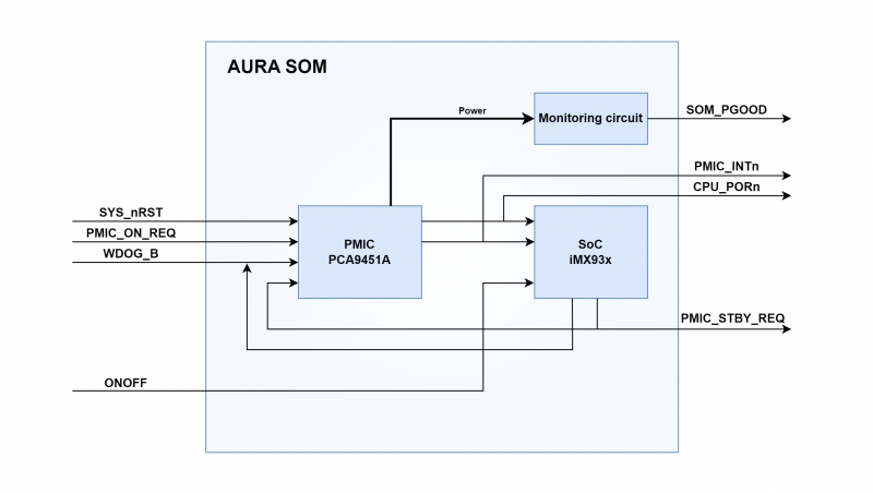
AURA SOM simplifies this task by embedding all the needed circuitry. The following picture shows a simplified block diagram of PSU/voltage monitoring circuitry:
The PSU is composed of two main blocks:
- power management integrated circuit (PMIC)
- additional generic power management circuitry that completes PMIC functionalities.
The PSU:
- generates the proper power-up sequence required by the SoC, surrounding memories, and peripherals
- synchronizes the powering up of carrier board's circuitry to prevent back powering.
Power-up sequence[edit | edit source]
The typical power-up sequence is the following:
- VIN_SOM (+3.3V) main power supply rail is powered.
- CPU_PORn (active-low) is driven low by PMIC; PMIC initiates power-up sequence needed by iMX93x processor.
- SOM_PGOOD goes up when all SoC, memories, and I/O power rails are ready.
- Finally PMIC releases CPU_PORn; this signal brings the processor out of reset.
Note on SOM_PGOOD usage[edit | edit source]
SOM_PGOOD is generally used on carrier board to drive loads such as DC/DC enable inputs or switch on/off control signals in order to prevent back power.
Depending on the kind of such loads, SOM_PGOOD might not be able to drive them properly. On AURA SOM this signal is driven by a push-pull output at NVCC_3V3 rail, with max 20 mA output current.
Note on CPU_PORn[edit | edit source]
Internally to the SOM, CPU_PORn is pulled-up with 100 kOhm.
Reset scheme and control signals[edit | edit source]
The following picture shows the simplified block diagram of the reset scheme, power control signals and voltage monitoring.
|
As depicted in the previous picture, only two external sources are required: SYS_nRST and (optionally) WDOG_B. In case of low power usage, the ONOFF signal can be used. The other generates reset signals may be used for driving properly the carrier's board circuitry. |
Signal description[edit | edit source]
AURA SoM provides the following reset signals:
- SYS_nRST to performs a PMIC reset (cold or warm reset depends on PIMIC configuration register)
- WDOG_B to performs a PMIC reset (cold or warm reset depends on PIMIC configuration register)
- CPU_PORn to force memories and peripherals to reset, in order to bring them in a known condition
with some related control signals:
- SOM_PGOOD to turn on circuitry external to the SoM
- PMIC_INTn to manage PMIC register interrupts
provides this power control signal:
- ONOFF to turn the SoC off and on in case of low power use
and provides these monitor signals:
- PMIC_ON_REQ used internally to start a PMIC power sequence, so that reboot the SoC
- PMIC_STBY_REQ used internally to generate proper power for the SoC in sleep mode
The electrical and functional characteristics of these signals are listed in the following table:
| Signal | Type | Driven | Affect | Purpose | |
|---|---|---|---|---|---|
| SYS_nRST | Open drain,
User input |
PMIC Input,
pulled-up inside the PMIC |
Externally | PMIC | PMIC performs cold reset (warm reset can be set from configuration register) when SYS_nRST is asserted low. |
| WDOG_B | Open drain,
User input |
PMIC Input,
pulled-up with 100 kohm inside the SoM |
Externally or SoC | PMIC | PMIC performs cold reset (warm reset can be set from configuration register) when WDOG_B is asserted low. |
| CPU_PORn | Open drain,
User output |
PMIC Output, open drain
pulled-up with 100 kohm inside the SoM |
PMIC | SoC, onboard eMMC and PHY ETH, External | Reset memories and peripherals internal and external to the SoM after a power-on sequence. This guarantees it is in a known state when reset signal is released. |
| SOM_PGOOD | Push pull,
User output |
Monitor Output, 3V3 LVTTL | SoM | External | Turn on the external circuitry of the SoM when the SoC's power is ready, in order to prevent backpower. |
| PMIC_INTn | Open drain,
User output |
PMIC Output, open drain
pulled-up with 10 kohm inside the SoM |
PMIC | SoC and External | PMIC_INTn is asserted low when an interrupt bit status in PMIC's register is changed. |
| ONOFF | Open drain,
User input |
SoC Input,
pulled-up with 100 kohm inside the SoM |
Externally | SoC | SoC switches from low-power mode to run mode (or vice versa) when ONOFF is asserted low (kernel-definable modes, distinguished by short or long press). The main power must remain active so that some data can be stored even if the processor is turned off. See Battery-Backed Secure Memory (BBSM) on reference manual. |
| PMIC_ON_REQ | User monitor | PMIC Input,
pulled-down with 100 kohm inside the SoM |
SoC | PMIC | PMIC starts power on sequence when PMIC_ON_REQ is asserted high. |
| PMIC_STBY_REQ | User monitor | PMIC Input,
pulled-down with 100 kohm inside the SoM |
SoC | PMIC | PMIC enters in standby mode when PMIC_STBY_REQ is asserted high.
This allows the SoC to enter sleep mode. |
Handling CPU-initiated software reset[edit | edit source]
By default, i.MX93 processor does not assert any external signal when it initiates a software reset sequence. Furthermore, the default implementation of software reset, like other reset sources, initiates a complete power sequence except for the BBSM rail: all non BBSM registers are reset.
This technique is implemented in DESK-MX9-L. At the software level, U-Boot and Linux kernel software reset routines make use of the processor's WDT #1 to assert the WDOG1_WDOG reset signal. This signal in turn is routed to WDOG_ANY pad (MUX mode ALT_0). At the hardware level, this signal is connected to the WDOG_B PMIC pin driving a PMIC reset.
System boot[edit | edit source]
|
This page illustrates the characteristics of the AURA's boot subsystem. Reading of the chapter System Boot of the i.MX 93 Applications Processor Reference Manual is highly recommended [1], though. i.MX93 SOC features several options in terms of booting. Such options are detailed in that document |
By default, AURA supports Single Boot modes (i.e. the Cortex-A55 is the boot core) as detailed in the rest of the document. Other options are available on-demand, however, allowing the implementation of different configurations. DAVE Embedded Systems' team is available for additional information on this matter. If necessary, please contact sales@dave.eu.
The boot process begins at Power On Reset (POR) where the hardware reset logic forces the ARM Cortex-A55 core to begin execution starting from the on-chip boot ROM. The boot ROM:
- determines whether the boot is secure or non-secure
- performs some initialization of the system and clean-ups
- reads the mode pins to determine the primary boot device
- once it is satisfied, it executes the boot code
Boot options[edit | edit source]
The default primary boot device is defined at the factory and identified by the 'Boot Mode' field of the ordering code as follows:
- 0: SPI NOR / SD option (SOM code: DAUxxx0xxxxR)
- 1: eMMC / SD option (SOM code: DAUxxx1xxxxR)
- 2: SPI NAND / SD option (SOM code: DAUxxx2xxxxR)
For both options an alternative primary boot from SD/MMC card is provided, selectable by driving low the BOOT_MODE_SEL signal. Bootable SD/MMC card connects via the SD2 (USDHC2) bus.
All boot modes provide 'single boot' mode, meaning that the Cortex-A55 is the first core to boot. In any case, boot process is managed by on-chip boot ROM code that is described in detail in processor's Reference Manual.
| Ordering code 'Boot Mode' fileld | BOOT_MODE_SEL | Primary boot device |
|---|---|---|
| 0 | 0 | SD/MMC card on USDHC2 |
| 1 | FlexSPI NOR on FLEXSPI1 | |
| 1 | 0 | SD/MMC card on USDHC2 |
| 1 | eMMC on USDHC1 | |
| 2 | 0 | SD/MMC card on USDHC2 |
| 1 | FlexSPI NAND on FLEXSPI1 |
Note on boot signals[edit | edit source]
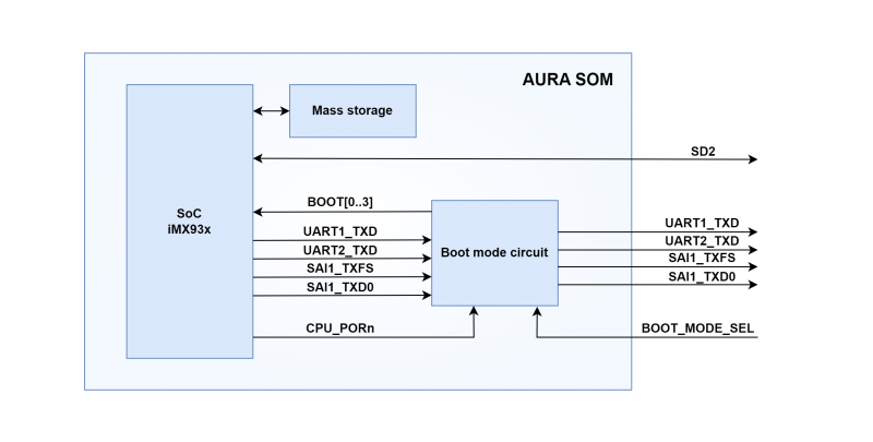
- BOOT_MODE_SEL is latched when processor reset CPU_PORn is released. Inside the SOM, BOOT_MODE_SEL is pulled-up with 10 kohm.
- The iMX93x SoC uses some GPIOs to read the boot configuration set on the SOM: for this reason the SOM's ports UART1_TXD, UART2_TXD, SAI1_TXFS and SAI1_TXD0 are floating (high impedance) while CPU_PORn signal is low.
Note on boot[edit | edit source]
In case no valid image is found in primary boot device, boot ROM shall enable USB serial download mode automatically on USB OTG1.
Important note for manufacture mode management[edit | edit source]
When the internal boot and recover boot (if enabled) failed, the boot goes to the SD/MMC manufacture mode before the serial download mode.
By default, the SD/MMC manufacture mode is enabled. DAVE Embedded Systems do not blow the fuse of the DISABLE_SDMMC_MFG in order to disable it.
Boot ROM detects SD/MMC card on USDHC2 port. If a card is inserted, ROM will try to boot from it. SD2_CD_B is used as card detect signal during bootrom's manufacture mode. This signal need to be kept high during bootstrap stage to prevent the intervention of bootrom's manufacture mode, if it's not desidered.
Bootstrap stage has to be intended as the time elapsing between the release of hardware reset (CPU_PORn) and the execution of the first instruction of user code (typically this is the reset vector of U-Boot boot loader).
References[edit | edit source]
[1] NXP, i.MX 93 Applications Processor Reference Manual
JTAG[edit | edit source]
JTAG signals are routed to the J1 primary connector of the AURA PCB. See the pinout section for more details.
Peripherals[edit | edit source]
Peripheral Audio[edit | edit source]
The Audio interface available on AURA is based on i.MX93 SoC. The audio port supports the following standards and features:
- Synchronous Audio Interface (SAI)
- Pulse Density Modulated Microphone Interface (PDM)
- Sony/Philips digital interface (SPDIF XCVR)
- Medium Quality Sound (MQS) (MQS is used to generate medium quality audio to connect stereo speakers or headphones to a power amplifier)
Description[edit | edit source]
The Synchronous Audio Interface (SAI) supports 2 Tx lanes and 2 Rx lanes
- 16-word TX/RX FIFO and up to 32 words per frame
- One set of Tx clocks and frame sync
The SPDIF (Sony Philips Digital Interface) Transceiver supports raw capture mode that can save all the digital audio bits into audio buffer.
The PDM (Pulse Density Modulated Microphone Interface) module receives audio from a microphone. It includes the following features:
- Supports up to 8-microphones (4 lanes)
- Supports frame synchronization
The MQS (Medium Quality Sound) is used to generate medium quality audio via a standard GPIO. It provides only simple audio reproduction. Stereo speakers or headphones can be connected to a power amplifier without an additional DAC chip.
- 2-channel, LSB-valid 16 bit, MSB shift-out first serial data (sdata)
- Signals over 10 kHz have worse THD+N values
Pin mapping[edit | edit source]
The Pin mapping is described in the Pinout table section
Peripheral CAN[edit | edit source]
The CAN interface available on AURA is based on i.MX93 SoC. The SOC includes two instances of CAN-FD Controllers (CAN-FD1 is in AONMIX and CAN-FD2 is in WAKEUPMIX).
The FlexCAN module is a full implementation of the CAN with Flexible Data Rate (CAN FD) protocol specification and CAN protocol specification, Version 2.0 B compliant with the ISO 11898-1:2015 standard
Description[edit | edit source]
The FlexCAN module includes these distinctive features:
- Flexible mailboxes configurable to store 0 to 8, 16, 32, or 64 bytes data length
- Each mailbox configurable as receive or transmit, all supporting standard and extended messages
- Individual Rx Mask registers per mailbox
- Full-featured
- legacy Rx FIFO with storage capacity for up to six frames and automatic internal pointer handling with DMA support
- enhanced Rx FIFO with storage capacity for up to 20 CAN FD frames
- Transmission abort capability
- Flexible message buffers (MBs), totaling 96 message buffers of 8 bytes data length each, configurable as Rx or Tx
- Programmable
- Loop-Back mode supporting self-test operation
- Programmable transmission priority scheme: lowest ID, lowest buffer number, or highest priority
- Time stamp based on 32-bit free running timer, with an optional external time tick
- Short latency time due to an arbitration scheme for high-priority messages
- Low power modes, with programmable wakeup on bus activity
- Powerful
- legacy Rx FIFO ID filtering, capable of matching incoming IDs against either 128 extended, 256 standard, or 512 partial (8 bit) IDs, with up to 32 individual masking capability
- Enhanced Rx FIFO ID filtering, capable of matching incoming IDs against either 64 extended or 128 standard ID filter elements with three filtering schemes: mask + filter, range, and two filters without mask
Pin mapping[edit | edit source]
The Pin mapping is described in the Pinout table section
Peripheral Ethernet[edit | edit source]
AURA SOM is based on i.MX93 SoC which includes two 10/100/1000Mbps Ethernet interfaces.
- 1G-bit Ethernet QoS with TSN support
- 1G-bit Ethernet with AVB support
Description[edit | edit source]
The first Ethernet port has a EQoS-TSN module and supports the following standards and features:
- compliance with IEEE802.3-2015 specifications. It can support advanced applications such as Time-Sensitive Networking (TSN) and Audio Video Bridge (AVB)
- Time aware shaper (IEEE802.1Qbv), Time synchronization (IEEE1588-2008), and Frame pre-emption (IEEE802.1Qbu) for Time-Sensitive Networking (TSN)
- Media clock recovery and generation for AVB
- RMII specification version 1.2
- RGMII specification version 2.6
- Flexibility to control the Pulse per second (PPS) output signal
- VLAN insertion, replacement and deletion in transmitted packets with per-packet or static-global control
- Insertion, replacement and deletion of up to two VLAN tags
- Insertion, replacement and deletion of queue/channel based VLAN tags
- IEEE802.1Q VLAN tag detection and option to delete from received packets
- Flexible address filtering modes
- Additional packet filtering
The second Ethernet port supports the following standards and features:
- compliance with the IEEE802.3-2002 standard (full 802.3 specification with preamble/SFD generation, frame padding generation, CRC generation and checking)
- Dynamically configurable to support 10/100-Mbit/s and gigabit operation
- 10/100 Mbit/s full-duplex and configurable half-duplex operation and gigabit full-duplex operation
- VLAN-tagged frames according to IEEE 802.1Q
- AVB (Audio Video Bridging, IEEE 802.1Qav)
- credit-based bandwidth distribution policy can be combined with time-based shaping
- AVB endpoint talker and listener support
- arbitration between different priority traffic (for example, AVB class A, AVB class B, and non-AVB)
- all IEEE 1588 frames with 4-channel IEEE 1588 timer (each channel supports input capture and output compare using the 1588 counter)
Pin mapping[edit | edit source]
The Pin mapping is described in the Pinout table section
Peripheral MIPI[edit | edit source]
The AURA SOM based on i.MX93 SoC has two MIPI interfaces:
- One 4-lane MIPI-DPHY DSI Tx PHY and MIPI-DSI Controller
- One 2-lane MIPI-DPHY CSI Rx PHY and MIPI-CSI Controller compliant to MIPI-DSI specification v1.2 and MIPI-DPHY specification v1.2
Description[edit | edit source]
The MIPI-DSI controller supports the following features:
- Configurable selection of system interfaces:
- AMBA APB for control and optional support for Generic and DCS commands
- Display Pixel Interface (DPI) for Video mode interface (optional)
- Fault recovery mechanisms
- Ultra Low-Power mode with PLL disabled
- DPI features:
- DPI signals programmable polarity
- Extended resolutions beyond the DPI standard
- Maximum resolution limited by available DSI physical link bandwidth, which is determined by the number of physical (up to 2048x1080@60Hz 24bpp with 4 lanes)
lanes and the maximum speed that they can achieve
- Video pattern generator
The MIPI CSI-2 controller receives data from a CSI-2 compliant camera sensor and supports the following blocks:
- PHY-Protocol Interface (PPI) Data Processor and Pattern Generator
- De-scrambler
- PHY Adaptation Layer
- Image Pixel Interface (IPI) Controller (48-bit parallel bus operating at pixel clock rate)
- Two operating modes: Camera Timing and Controller Timing
- Generates pixel stream (48 or 16 bit modes)
- data formats: YUV, RGB, RAW, User defined
Pin mapping[edit | edit source]
The Pin mapping is described in the Pinout table section
Peripheral LVDS[edit | edit source]
Description[edit | edit source]
The LVDS interface available on AURA is based on i.Mx93 SoC and supports the following standards and features:
- compliance to the EIA-644-A standard
- 4-lane LVDS display (up to 1366x768 or 1280x800)
- two mapping standards: SPWG and JEIDA mapping
Pin mapping[edit | edit source]
The Pin mapping is described in the Pinout table section
Peripheral LCD[edit | edit source]
The LCD interface available on AURA is based on i.Mx93 SoC and fetches graphics stored in memory and display them on a TFT LCD panel.
Description[edit | edit source]
The LCD port supports the following standards and features:
- Parallel display (up to 1366x768 or 1280x800)
- The display mode supports DOTCLK mode only
• One layer can support the programmable plane size(Width/Height/Pitch) on the panel
The LCD interface may be driven by a Pixel Processing Pipeline (PXP) used to process graphics buffers or composite video and graphics data before sending to an LCD display.
The PXP combines the following into a single processing engine:
- Scaling: YUV 422, 420, 444 and any RGB formatted pixels
- Color Space Conversion (CSC): converting from YUV to RGB
- Secondary Color Space Conversion (CSC2)
- Rotation: 0, 90, 180, 270 degrees and vertical/horizontal flips
- Composite Alpha Blending and Color Key
Pin mapping[edit | edit source]
The Pin mapping is described in the Pinout table section
LCD pins table mapping[edit | edit source]
The following table lists the LCD interface pads mapped to the AURA SO-DIMM pads:
| LCD signal | IO PAD | SO-DIMM pin | Notes |
|---|---|---|---|
| PCLK | GPIO_IO00 | 179 | |
| DE | GPIO_IO01 | 183 | |
| VSYNC | GPIO_IO02 | 195 | |
| HSYNC | GPIO_IO03 | 181 | |
| D[0] | GPIO_IO04 | 80 | |
| D[1] | GPIO_IO05 | 78 | |
| D[2] | GPIO_IO06 | 43 | |
| D[3] | GPIO_IO07 | 40 | |
| D[4] | GPIO_IO08 | 49 | |
| D[5] | GPIO_IO09 | 47 | |
| D[6] | GPIO_IO10 | 55 | |
| D[7] | GPIO_IO11 | 59 | |
| D[8] | GPIO_IO12 | 191 | |
| D[9] | GPIO_IO13 | 193 | |
| D[10] | GPIO_IO14 | 89 | |
| D[11] | GPIO_IO15 | 91 | |
| D[12] | GPIO_IO16 | 66 | |
| D[13] | GPIO_IO17 | 34 | |
| D[14] | GPIO_IO18 | 45 | |
| D[15] | GPIO_IO19 | 68 | |
| D[16] | GPIO_IO20 | 72 | |
| D[17] | GPIO_IO21 | 36 | |
| D[18] | GPIO_IO22 | 74 | |
| D[19] | GPIO_IO23 | 76 | |
| D[20] | GPIO_IO24 | 46 | |
| D[21] | GPIO_IO25 | 42 | |
| D[22] | GPIO_IO26 | 70 | |
| D[23] | GPIO_IO27 | 44 |
Peripheral SDIOs[edit | edit source]
The Ultra Secured Digital Host Controller (uSDHC) provides the interface between the host system and the eMMC, SD card, and SDIO. The SDIO interfaces available on AURA are based on iMX93 SoC.
AURA SOM provides up to three SDIO interfaces available for an external memory device connection:
- the SD1 interface is used for the on board eMMC flash (but it is optionally available on the SO-DIMM connector)
- the SD2 interface is available on the SO-DIMM connector
- the SD3 interface is optionally for the on board SPI flash (otherwise it is available on the SO-DIMM connector)
Description[edit | edit source]
The SDIOs port supports the following standards and features:
- Conforms to the SD Host Controller Standard Specification version 2.0/3.0
- Compatible with the eMMC System Specification version 4.2/4.3/4.4/4.41/4.5/5.0/5.1
- Compatible with the SD Memory Card Specification version 3.0 and supports the Extended Capacity SD Memory Card
- Compatible with the SDIO Card Specification version 2.0/3.0
- Supports 1-bit/4-bit SD and SDIO modes, and 1-bit/4-bit/8-bit MMC modes
- Card bus clock frequency up to 208 MHz
Pin mapping[edit | edit source]
The Pin mapping is described in the Pinout table section
Peripheral USB[edit | edit source]
The two USB interfaces available on AURA are based on iMX93 SoC which includes two instances of USB 2.0 Controllers and PHY that can be used as USB OTG port, USB Host port or USB Device port.
Universal Serial Bus (USB) is an industry-standard that establishes specifications for cables and connectors and protocols for connection, communication and power supply (interfacing) between computers, peripherals and other computers.
Description[edit | edit source]
There are two USB 2.0 controller cores in this chip:
- Controller Core 0 is also named USB1
- Controller Core 1 is also named USB2
Both USB 2.0 Controllers provide the following features:
- High-Speed/Full-Speed/Low-Speed (HS/FS/LS) OTG core
- HS/FS/LS UTMI compliant interface
- HS, FS, and LS operation in HOST mode (with UTMI transceiver)
- HS and FS operation in Peripheral mode (with UTMI transceiver)
- Hardware support for OTG signaling, session request protocol, and host negotiation protocol
- 8 bidirectional endpoints
VBUS detection[edit | edit source]
On the AURA external connector, the USB[1..2]_VBUS pins are present to detect that the USB is enabled end therefore power the internal USB PHY.
Pin mapping[edit | edit source]
The Pin mapping is described in the Pinout table section
Peripheral SPI[edit | edit source]
A SPI bus is a synchronous serial communication interface used in embedded systems. It is typically used to perform short-distance communications between microcontrollers and peripheral devices.
The SPI interface available on AURA is based on i.MX93 SoC. The chip includes eight instances of LPSPI Modules:
- LPSPI1 and LPSPI2 are in Low Power Real Time Domain
- LPSPI[3..8] are in Application Flex Domain
- SPI1 and SPI2 are only supported in Master Mode, not Slave Mode.
Description[edit | edit source]
The SPI port supports the following standards and features:
- FIFO register access supported by DMA transmit and receive requests
- Continues operating in Stop mode, if configured to do so and an appropriate clock is available
- 32-bit word size
- Configurable clock polarity and phase
- Master mode—supports 2 peripheral chip selects and Slave mode
- 8-word transmit, receive and command FIFO
- Flexible timing parameters in Master mode, including SCK frequency and duty cycle, and delays between PCS and SCK edges
- Continuous transfer option to keep PCS asserted across multiple frames
- Full-duplex transfers support 1-bit transmit and receive on each clock edge and Half-duplex transfers support
Pin mapping[edit | edit source]
The Pin mapping is described in the Pinout table section
Peripheral I2C[edit | edit source]
LPI2C is a low-power Inter-Integrated Circuit (I2C) module that supports an efficient interface to an I2C bus as a controller and/or as a target.
The I2C interface available on AURA is based on i.MX93 SoC. The chip includes eight instances of LPI2C Modules:
- LPI2C1 and LPI2C2 are in Low Power Real Time Domain
- LPI2C[3..8] are in Application Flex Domain
Description[edit | edit source]
The LPI2C port supports the following standards and features:
- Compliance with the System Management Bus (SMBus) Specification, version 3
- Standard, Fast, Fast+ and Ultra Fast modes
- High-speed mode (HS) in target mode
- Multi-controller, including synchronization and arbitration
- Clock stretching
- General call, seven-bit addressing, and ten-bit addressing
- Software reset, START byte, and Device ID
The LPI2C controller supports:
- Command/transmit/receive FIFO of 8 words (8-bit transmit data + 3-bit command or 8-bit receive data)
- Command FIFO waits for idle I2C bus before initiating transfer.
- Flags and optional interrupt signals at repeated START condition, STOP condition, loss of arbitration, unexpected NACK, and command word errors
- Configurable bus idle timeout and pin-stuck-low timeout.
The LPI2C target supports:
- Separate I2C target registers
- 7-bit or 10-bit addressing, address range, SMBus alert, and general call address
- Transmit/Receive data register that supports interrupt or DMA requests
- Software-controllable ACK or NACK, with optional clock stretching on ACK/NACK bit
- Configurable clock stretching
- Flags and optional interrupt at end of packet, STOP condition, or bit error detection
Pin mapping[edit | edit source]
The Pin mapping is described in the Pinout table section
Peripheral I3C[edit | edit source]
The MIPI Alliance Improved Inter-Integrated Circuit (MIPI I3C) improves upon the use and power of I2C, and provides an alternative to SPI for mid-speed applications.
The I3C interface available on AURA is based on i.MX93 SoC. The chip includes two instances of I3C Modules:
- I3C1 is in Low Power Real Time Domain
- I3C2 is in Application Flex Domain
Description[edit | edit source]
The I3C bus protocol supports:
- all required and most optional features of the MIPI Alliance Specification for I3C, v1.0 and v1.1, except for ternary data rates (HDR-TSP and HDR-TSL)
- In-band interrupts (IBI)
- Common Command Codes (CCC)
- Dynamic addressing
- Multi-controller/multi-drop
- Hot-Join (HJ)
- I2C compatibility
Pin mapping[edit | edit source]
The Pin mapping is described in the Pinout table section
Peripheral UART[edit | edit source]
LPUART provides asynchronous, serial communication capabilities with external devices. LPUART can continue operating when the processor is in Low-Power mode, if an appropriate peripheral clock is available.
The UART interface available on AURA is based on i.MX93 SoC. The chip includes eight instances of UART Modules:
- LPUART1 and LPUART2 are in Low Power Real Time Domain
- LPUART[3..8] are in Application Flex Domain
Description[edit | edit source]
The UART port supports the following standards and features:
- Full-duplex, standard NRZ format
- Programmable baud rates (13-bit modulo divider) with a configurable oversampling ratio
- Asynchronous operations of transmit and receive baud rates with respect to the bus clock
- Interrupt, DMA, or polled operations
- Hardware parity generation and checking
- Programmable 7-bit, 8-bit, 9-bit, or 10-bit character length
- Programmable 1-bit or 2-bit stop bits
- Hardware flow control support for request to send (RTS) and clear to send (CTS) signals
- Selectable IrDA 1.4 return-to-zero-inverted (RZI) format with a programmable pulse width
Pin mapping[edit | edit source]
The Pin mapping is described in the Pinout table section
Peripheral ADC[edit | edit source]
The ADC module available on AURA is based on i.MX93 SoC. The SOC has one instance of the ADC module: it is an 8-channel 12-bit 1MS/s ADC with 4 channels connected to pins in the package. It has its own dedicated pads and is not muxed with GPIO.
Description[edit | edit source]
The ADC port supports the following features:
- Successive Approximation Register (SAR) method
- 4-channel, 12-bit resolution
- Multiple modes of starting conversion (Normal, Injected)
- Software-initiated conversions in Normal and Injected modes, or external hardware trigger
- Programmable DMA enables for each channel
- Programmable presampling for channels
- Programmable clock prescaler
- Software-initiated calibration
Pin mapping[edit | edit source]
The Pin mapping is described in the Pinout table section
Peripheral FlexIO[edit | edit source]
FLEXIO uses shifters, timers, and external triggers to shift data into or out of the FLEXIO. It is a a highly configurable module providing a wide range of functionality, including:
- Emulation of various serial or parallel communication protocols
- Flexible 16-bit timers with support for various trigger, reset, enable, and disable conditions
The FlexIO module available on AURA is based on i.MX93 SoC. The Flexible I/O (FLEXIO) is a highly configurable module providing a wide range of functionality.
Description[edit | edit source]
The FlexIO module supports the following features:
- Array of 32-bit shift registers with transmit, receive, data match, logic, and state modes
- Double-buffered shifter operation for continuous data transfer
- Shifter concatenation to support large transfer sizes
- Automatic start and stop bit generation
- 1, 2, 4, 8, 16, or 32 multi-bit shift widths for parallel interface support
- Interrupt, DMA, or polled transmit and receive operation
- Programmable baud rates independent of bus clock frequency
- Highly flexible 16-bit timers with support for various internal or external trigger, reset, enable, and disable conditions
- Programmable logic mode
- Programmable state machine for offloading basic system control functions from CPU
- Integrated general-purpose input/output registers and pin rising or falling edge interrupts
- Support for a wide range of protocols, including but not limited to:
- UART, I2C, SPI, I2S, Camera IF, Motorola 68K or Intel 8080 bus, PWM or waveform generation
Pin mapping[edit | edit source]
The Pin mapping is described in the Pinout table section
Peripheral Real Time Clock[edit | edit source]
The Real Time Clock is part of i.MX93 SoC Battery Backed Secure Module (BBSM).
Description[edit | edit source]
The Real Time Clock supports the following features:
- Can be driven by an independent clock source (other than the clock that the SoC uses)
- Clock counter does not roll over: the RTC Alarm Register represents the number of seconds, and supports time alarm as high as ~140 years
- Has a programmable timed interrupt: the RTC Alarm (from BBSM) is mapped as an interrupt to NVIC and GIC
- The RTC alarm is also a wake-up source from any low power modes
- The Secure Real Time Clock continues counting when SoC power is off
Peripheral Watchdog[edit | edit source]
WDOG is an independent timer that is available for system use. It provides a safety feature to ensure that the software is executing as planned and that the CPU is not stuck in an infinite loop or executing unintended code.
The Watchdog module available on AURA is based on i.MX93 SoC. The SOC has five WDOG timers:
- WDOG1 and WDOG2 are reset whenever the Cortex-M33 is reset
Description[edit | edit source]
The WDOG port supports the following features:
- Configurable clock source inputs independent of the bus clock
- Programmable 16-bit timeout value
- Window mode option for the refresh mechanism
- Optional timeout interrupt to allow post-processing diagnostics
- Write-once-after-reset configuration fields
Pin mapping[edit | edit source]
The Pin mapping is described in the Pinout table section
Peripheral Security[edit | edit source]
The Security module available on AURA is based on i.MX93 SoC. The security functions to protect systems against physical and network attacks. Fine-grained key management capabilities are augmented by extensive crypto services for advanced attack resistance.
Description[edit | edit source]
The chip security system includes the following features:
- Edgelock secure enclave as a hardware root of trust
- Secure Boot: Advanced High Assurance Boot (AHAB) feature in the system boot
- Secure Debug allows customers to securely develop and debug software during development or deployment in the field and Secure Life cycle Management
- Crypto: On-the-fly decryption
- Tamper Detection: Battery Backed Secure Module (BBSM) with Secure Real Time Clock
- Trusted Resource domain controller (TRDC)
Electrical, Thermal and Mechanical Features[edit | edit source]
Operational characteristics[edit | edit source]
Maximum ratings[edit | edit source]
| Parameter | Min | Typ | Max | Unit |
|---|---|---|---|---|
| Main power supply voltage | -0.3 | 3.3 | 3.6 | V |
Recommended ratings[edit | edit source]
| Parameter | Min | Typ | Max | Unit |
|---|---|---|---|---|
| Main power supply voltage | 3.135 | 3.3 | 3.465 | V |
Power consumption[edit | edit source]
Inevitably, system integrators face a number of challenges when designing a product that includes a SOM. These usually involve managing heat produced by the devices and sizing the carrier PSU.
To help them, AURA SoM power measurements are provided considering several use cases. Please note that AURA platform is so flexible that it is virtually impossible to test for all possible configurations and applications on the market. The use cases presented here should cover many realistic scenarios, however. Hence, they are supposed to be a useful and thorough reference. Of course, the actual customer's application may differ significantly with respect to the ones considered here. For this reason, application-specific requirements should always taken into account when designing such systems. Further measurements on a real system emulating the final product and/or simulations are recommended options as well.
Definitions[edit | edit source]
For convenience, some of the definitions established by NXP for SOC operating modes are reported below (for more details, please see also AN13917 chapter 4.2):
- Run mode: in this mode, the Cortex-A55 CPU is active and running. Some portions can be shut off for power saving. It is possible with the NXP Low Drive system to scale frequency and voltage to balance between performance and consumption (see this page):
- Over drive (OD mode) with processor that works at 1.7 GHz and VDD_SOC at 0.9 V, DRAM works at 3733 MT/s
- Nominal drive (ND mode) with processor that works at 1.4 GHz and VDD_SOC at 0.85 V, DRAM works at 2800 MT/s
- Low drive with processor that works at 933 MHz and VDD_SOC at 0.8 V, DRAM works at 1866 MT/s
- Low drive with SWFFC (Software Fast Frequency Change) with processor that works at 933 MHz and VDD_SOC at 0.8 V, DRAM works at 625 MT/s
- Low-power mode: this mode is defined as a Low-power run mode with all external power rails on. In this mode, all unnecessary power domains (MIX) can be off. The AONMIX and internal modules, such as OSC24M/PLL, are an exception in this mode. The Cortex CPU in AONMIX handles all the computing and data processing. Cortex-A55 is powered down and DRAM can be in self-refresh/retention mode.
- Idle mode: this mode is defined as one that a CPU can enter automatically when no threads are engaged, and no high-speed devices are in use. CPU can be put into a power-gated state, but with L3 data retained, DRAM, and bus clocks are reduced. Most of the internal logic is clock-gated; yet is still powered. In this mode, all the external power from PMIC remains the same, and most IPs remain in their state. Therefore, the interrupt response in this mode is quick compared to the Run mode.
- Suspend mode: this mode is defined as the most power-saving mode since it shuts off all the clocks and all the unnecessary power supplies. In this mode, the Cortex-A55 CPU is fully power gated, all internal digital logic, and the analog circuits that can be powered down are off, and all PHYs are power gated. VDD_SOC (and related digital supply) voltage is reduced to the "Suspend mode" voltage. Compared to Idle, this mode takes a longer time to exit, but it also uses far less energy.
- BBSM mode: this mode is also called RTC mode. In this mode, to keep RTC and BBSM logic alive, only the power for the BBSM domain remains on.
- Off mode: in this mode, all power rails are off.
Testbench[edit | edit source]
Measurements were performed on a testbed composed as follows:
- INA226-based datalogger for power measurement
- AURA Evaluation Kit
- AURA Evaluation Kit with adapter only for stress user cases
- Linux BSP: DESK-MX9-L 5.1.0
W.r.t. the SoM, the model used was DAUC221000I0R SOM model:
- i.MX9352 1.7GHz (p.n. MIMX9352CVVXMAB)
- 2 GB LPDDR4 SDRAM
- 8 GB eMMC
For more information about software tools utilized for this testing, please refer to this page.
Power was measured on the SoM power rail 3.3VIN. The power was measured at 200 Sa/s for 3 minutes starting after the completion of the boot phase: the average, minimum, and maximum values found in each mode are shown in the following table while the corresponding time graphs are shown in the next paragraph.
Four major use cases have been considered:
- Run mode Cortex-A55 (light workload): after booting the Yocto Linux distribution, no additional user-space applications were executed other than the ones starting automatically such as
systemddaemons; please note, that all four drive modes were tested. - Run mode Cortex-A55 (heavy workload): in this configuration, to induce high consumption on A55 cores, the following energy-intensive operations were performed:
- both Ethernet interfaces were configured to operate at 1 Gbps and two instances of endless
iperf3processes were run (one for each interface) exchanging data with an external server - camera streaming a video to the HDMI display
- execute the
satapp for stressing the SOC and the SDRAM memory
- both Ethernet interfaces were configured to operate at 1 Gbps and two instances of endless
- Run mode Cortex-M33: the A55 cores were put into suspension, while M33 core run a test application
- Low-power modes: all cores are turned off; the three modes also turn off portions of the SoM and theSoC.
Linux user-space and bare metal applications[edit | edit source]
SAT(Stressful Application Test) for stressing the SoC and the RAM memory, https://github.com/stressapptest/stressapptestiperf3for stressing both ethernet interfaces, execute an endless with external server support, https://iperf.fr/gstreamerfor streaming camera to HDMI display, https://gstreamer.freedesktop.org/CoreMarkis provided by NXP as a prebuilt binary image for testing the M33 core: NXP AN13917 chapter 6.9, use case binaries.
Results[edit | edit source]
| ID | Mode group | Mode | Cortex A55 | Cortex M33 | SDRAM
[MT/s] |
VDD_SOC
[V] |
Power
[W] |
Notes | ||
|---|---|---|---|---|---|---|---|---|---|---|
| min | avg | max | ||||||||
| 1 | Run mode
(light workload) |
Over drive |
|
|
3733 | 0.90 | 1.601 | 1.696 | 2.211 | |
| 2 | Nominal |
|
|
2800 | 0.85 | 1.543 | 1.584 | 1.838 | ||
| 3 | Low drive |
|
|
1866 | 0.8 | 1.468 | 1.508 | 1.723 | ||
| 4 | Low drive with SWFFC
(Software Fast Frequency Change) |
|
|
625 | 0.8 | 1.415 | 1.462 | 1.610 | ||
| 5 | Run mode
(heavy workload) |
Over drive |
|
|
3733 | 0.90 | 2.030 | 2.443 | 2.779 |
|
| 6 | Nominal |
|
|
2800 | 0.85 | 1.808 | 2.023 | 2.209 | ||
| 7 | Low drive |
|
|
1866 | 0.8 | 1.625 | 1.834 | 2.001 | ||
| 8 | Low drive with SWFFC
(Software Fast Frequency Change) |
|
|
625 | 0.8 | 1.553 | 1.662 | 1.794 | ||
| 9 | Run mode | Over drive |
|
|
NA | 0.65 | 0.2739 | 0.2751 | 0.2777 |
|
| 10 |
|
|
NA | 0.65 | 0.2762 | 0.2780 | 0.2800 |
| ||
| 11 | Low-power modes | Idle |
|
|
NA | 0.65 | 0.5997 | 0.6043 | 0.6104 |
|
| 12 | Suspend |
|
|
NA | 0.65 | 0.1610 | 0.1636 | 0.1663 |
| |
| 13 | BBSM (Battery-Backed Secure Memory) |
|
|
NA | 0 | 820 x10-6 | 971 x10-6 | 1130 x10-6 |
| |
Power charts[edit | edit source]
The number between round brackets indicates the ID of the use case listed in the table above.
Run mode (light workload)[edit | edit source]
Run mode (heavy workload)[edit | edit source]
Run mode[edit | edit source]
Low-power modes[edit | edit source]
Considerations[edit | edit source]
As expected, low-power modes exhibit a quasi-static power consumption. On the contrary, the other modes show a dynamic component too.
References[edit | edit source]
- NXP AN13917, i.MX 93 Power Consumption Measurement, https://www.nxp.com/docs/en/application-note/AN13917.pdf
- NXP AN14022, i.MX 93 Migration Guide from i.MX 8M Nano, https://www.nxp.com/docs/en/application-note/AN14022.pdf
- NXP iMX93 datasheet, https://www.nxp.com/docs/en/data-sheet/IMX93CEC.pdf
- NXP iMX93 reference manual, https://www.nxp.com/webapp/Download?colCode=IMX93RM
Thermal management[edit | edit source]
The AURA SOM is designed to support the maximum available temperature range declared by the manufacturer.
The customer shall define and conduct a reasonable number of tests and verifications in order to qualify the DUT capabilities to manage the heat dissipation.
Any heatsink, fan etc shall be defined case by case.
DAVE Embedded Systems' team is available for any additional information, please contact sales@dave.eu.
Mechanical specifications[edit | edit source]
This chapter describes the mechanical characteristics of the AURA module.
Board Layout[edit | edit source]
The following figure shows the physical dimensions of the AURA module:
Connectors[edit | edit source]
The following figure shows the AURA connector layout:
CAD drawings[edit | edit source]
- DXF (2D):
- STEP (3D)
3D drawings[edit | edit source]
