ORCA SOM/ORCA Evaluation Kit/pdf
Getting started[edit | edit source]
Kit Identification Codes[edit | edit source]
The development kits are identified by a couple of codes:
- P/N Part Number identification code
- S/N Serial Number identification code
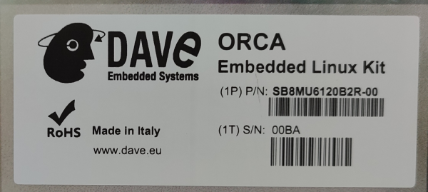
These codes are printed on a label stuck to the box containing the kit.
For example, the following picture shows such a label of an ORCA Evaluation Kit with Serial Number 00BA
These codes are required to complete the registration process of the kit.
Unboxing[edit | edit source]
Once you've received the kit, please open the box and check the kit contents with the packing list included in the box, using the table on this chapter as a reference.
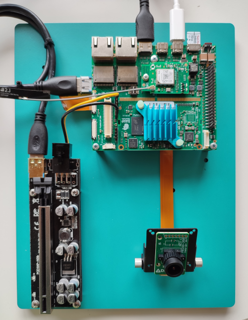
The hardware components (SOM, carrier boards and display) are pre-assembled, as shown in the picture below:
Video[edit | edit source]
Kit Contents[edit | edit source]
The following table list the kit components:
| Component | Description |
|---|---|
ORCA SBC
| |
| USB Type C Power Delivery wall mount adapter | |
| USB 3 with power delivery HUB | |
| USB C to USB C charging cable | |
| PCAM 5C camera module with flat FPC cable | |
| PCI-e riser card extension | |
| DWS Wifi and Bluetooth module | |
| FTDI TTL/USB cable (TTL-232RG-VIP-WE) | |
| Touchscreen Monitor, 8" 1280x720 (with power supply adapter and HDMI cable) | |
| Mini-HDMI to HDMI adapter | |
| MicroSDHC card |
Order codes[edit | edit source]
| Order code | Description |
|---|---|
| SB8MU6120B2R-00 | This code refers to the default configuration detailed above including SOM DMUE3300CxR |
microSD Layout[edit | edit source]
The microSD provided with the kit is used to store:
- a bootable partition (mmcblk0p1, vfat) containing:
- binary images (u-boot and kernel images)
- documentation
- DVDK virtual machine image
- root file system partition (mmcblk0p2, ext3)
Connections[edit | edit source]
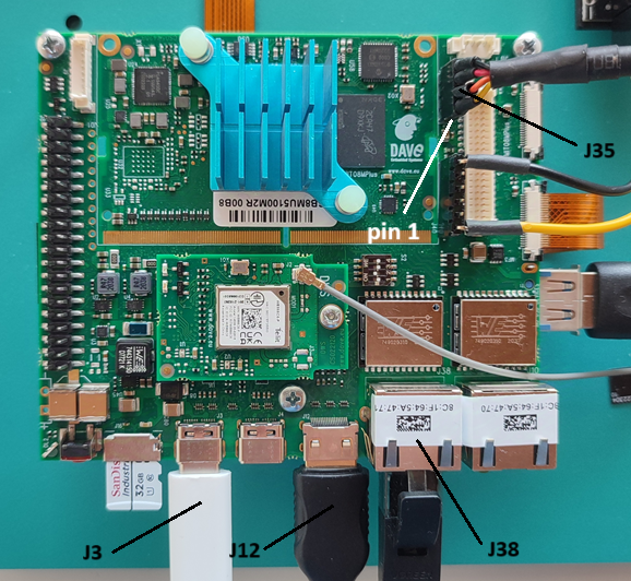
This section describes how to quick start the Evaluation Kit. The picture below shows the ORCA SBC inside into the Evaluation Kit:
The system is programmed to automatically boot Linux at power up, loading the bootloader, the kernel and device tree image and the root file system from the SD card memory.
To connect to the system:
- insert the SD card into the micro SD slot
- connect the USB Type C power adapter to J3 on the board
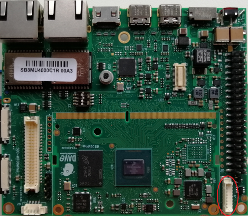
- connect the USB to TTL UART adapter to the J35 connector on the SBC and connect the USB side connector to an USB port on your computer
- if required, install the FTDI USB to serial driver
- start your favorite terminal emulator software on PC (eg: PuTTY, Minicom, ...); communication parameters are 115200,N,8,1
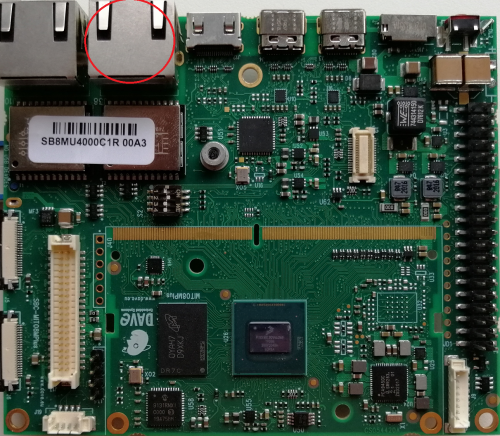
- (optional) connect the ethernet cable from your LAN hub/switch to the J38 (*)
eth0RJ45 connector- start SSH, using the following parameters:
- ip address: 192.168.0.89
- username: root
- empty password
- start SSH, using the following parameters:
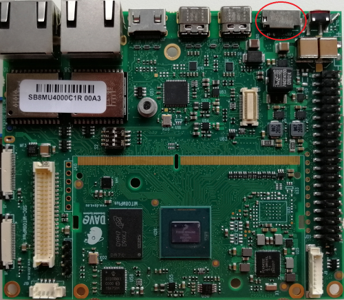
- (optional) connect the HDMI cable from your display monitor to the J12 connector (with the provided mini-HDMI to HDMI adapter)
|
Warning: please, pay attention to the debug cable header connection pin #1, see the picture here below |
(*)
|
Ethernet connector J38 has to be used as |
First boot[edit | edit source]
Once power has been applied, U-Boot bootloader will be executed and the debug messages will be printed on the serial console. U-Boot automatically runs the autoboot macro, that loads the kernel/dtb and launches it with the options for mounting the root file system from the SD card.
At the end of the boot process, a demo application is launched and you can interact with the system using the touchscreen. The Linux shell is available on the serial console. Moreover, both telnet and ssh services are available to connect to the system through the network.
Serial console[edit | edit source]
A simple Windows serial and SSH/telnet client and terminal can be downloaded from here.
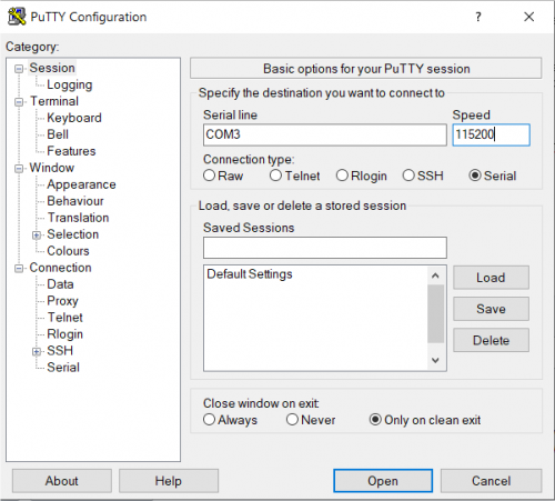
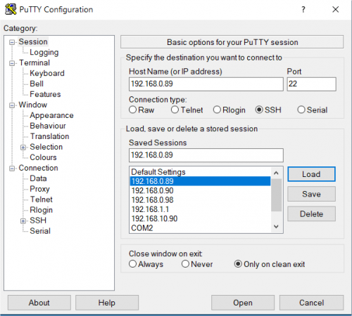
The following picture shows the serial setup for connecting to the EVK:
once selected the COM[x] serial port, click the Open button which starts the terminal. Once powered, the EVK shows the U-boot debug messages printed on the serial console.
Connecting through SSH[edit | edit source]
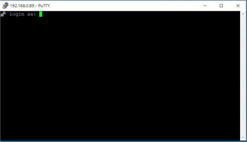
The following picture shows the SSH connection to the EVK:
once selected the IP address, click the Open button which starts the terminal. Once connected, the EVK shows the linux kernel prompt login for inserting the login:
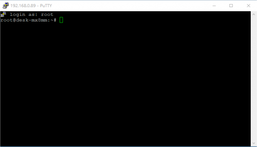
Then use the root login username without password:
Boot Configurations[edit | edit source]
ORCA Evaluation Board is built upon i.MX8M Plus SoC.
The following sections detail boot configuration options related to the ORCA SOM.
Available options[edit | edit source]
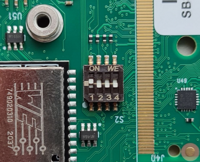
Boot modes can be selected by S2 switches which acts directly on SYSBOOT configuration pins.
S2 switches are connected to ORCA BOOT_MODE[3:0] pins allowing different boot modes.
where S2 switches are mapped as the following table:
| BOOT_MODE | S2 | Note |
|---|---|---|
| BOOT_MODE0 | S2.1 | |
| BOOT_MODE1 | S2.2 | |
| BOOT_MODE2 | S2.3 | |
| BOOT_MODE3 | unused |
| BOOT_MODE[3:0] | S2[4..1] | Boot sequence | Notes |
|---|---|---|---|
| 0000 | OFF-OFF-OFF-OFF | Boot From Internal Fuses | Please contact sales@dave.eu for more information |
| 0001 | OFF-OFF-OFF-ON | USB Serial Download | |
| 0010 | OFF-OFF-ON-OFF | USDHC3 | eMMC boot only, SD3 8-bit |
| 0011 | OFF-OFF-ON-ON | USDHC2 | SD boot only, SD2 microSD |
| 0100 | OFF-ON-OFF-OFF | NAND | 8-bit single device 256 page |
| 0101 | OFF-ON-OFF-ON | NAND | 8-bit single device 512 page |
| 0110 | OFF-ON-ON-OFF | QSPI | 3B read |
Reset Button[edit | edit source]
ORCA Evaluation Board has a pushbutton directly connected to the PMIC_RST_B signal which drives a SOM hardware reset.
S1 is the hardware reset button.
General Information[edit | edit source]
Product Highlights[edit | edit source]
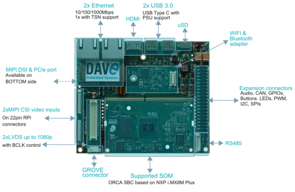
The ORCA SBC platform presented here provides a compact solution for any industry and can be easily interfaced with Plant Automation Control thanks to IEC-61131 SW language environment and/or other plug-ins like QT framework, Chromium web based GUI or multimedia GStreamer video applications.
The following table summarizes the main hardware and software features available with ORCA SBC:
Hardware[edit | edit source]
| Subsystem | Characteristics |
|---|---|
| CPU | NXP i.MX8M Plus |
| USB | Dual USB-C 3.0 ports |
| Serial Ports | RS232
RS485 with bus termination |
| Ethernet | Dual 10/100/1000Mbps with TSN |
| Display | Dual LVDS interface |
| Video | HDMI and MIPI interfaces |
| Camera | Dual MIPI-CSI intercaces up to 4 data lanes
with embedded ISP control |
| Audio | Dual SAI interfaces |
| Connectivity | Bluetooth and Wi-Fi |
| PSU | 12 to 24V DC, USB-C Power Delivery |
| Mechanical Dimensions | 87x103mm - Standard DIN (6modules) |
Software[edit | edit source]
| Subsystem | Options |
|---|---|
| Operating System | Linux, Android, FreeRTOS |
| Distribution | Yocto, Debian, Buildroot |
| Graphical Framework | Qt, Android, Chromium browser |
| Applications | SoftPLC, IoT runtime, nodeJS |
Block diagram[edit | edit source]
The following picture shows a simplified block diagram of the ORCA SOM Evaluation kit.
Main functional subsystems and interfaces are depicted.
The heart of the Evaluation Kit is the ORCA SOM module: please refer to the following Product Highlights page for the Evaluation Kit product highlights information.
Here below a summary for the main characteristics of the Kit.
Features Summary[edit | edit source]
| Feature | Specifications |
|---|---|
| Supported SOM | N.A. (embedded in the SBC) |
| Serial Ports | 1x UART RS232 on pin strip
1x UART RS485 on pin strip |
| Connectivity | 2x Gigabit Ethernet on RJ45 connectors 2x CAN port without PHY DWS Wireless module (optional) |
| Display | 2x LVDS
1x MIPI-DSI |
| Camera | 2x MIPI-CSI |
| Storage | 1x microSD slot |
| USB | 2x USB-C 3.0 port |
| Miscellaneous | GPIOs JTAG GROVE connector PCIe |
Electrical, Mechanical and Environmental Specifications[edit | edit source]
| Electrical / Mechanicals | Specifications |
|---|---|
| Supply voltage | + [12 - 24] V |
| Dimensions | 103 mm x 87 mm |
| Weight | 70.4 g |
| Operating Temperature | 0..70 °C |
Carrier board design guidelines[edit | edit source]
This page provides useful information and resources to system designers in order to design carrier boards hosting DAVE Embedded Systems system-on-modules (SOM).
These guidelines are provided with the goal to help designers to design compliant systems with DAVE Embedded Systems modules and they cover schematics and PCB aspects. They apply to several products that are listed on the top right corner of this page (see "Applies to" boxes).
Basic guidelines[edit | edit source]
In this section basic hardware guidelines valid for all DAVE Embedded Systems SOMs are detailed.
Schematics[edit | edit source]
- Check mirroring and pinout of DAVE Embedded Systems system-on-modules (SOM) connector
- Properly decouple DAVE Embedded Systems system-on-modules (SOM) power supply with large bulk capacitor and small bypass capacitor
- Use low-ESR X7R capacitor if possible
- Check for correct connection of TX and RX lines
- Add series resistors as interface needs (see interface details)
PCB[edit | edit source]
PCB Tecnology[edit | edit source]
Use a PCB technology as advised in the following table
| Parameter | Min | Typ | Max |
| Layers(number) | 4 | 6 | - |
| Power Plane Layers | 2 | 4 | - |
| Clearence(mils) | - | 6 | - |
| Trace Width(mils) | - | 6 | - |
| Vias hole (mechanical) | 0,3 | - | |
| Minimum number of via for each power signal layer changes | 2 | 3 | - |
| Minimum number of via for each power signal SOM connector pin | 1 | 2 | - |
| Component package size | - | 0603 | - |
| PCB Height(mm) | 1,4 | 1,6 | - |
- If vias smaller than minimum advised size are used, take care to maintain an adeguate number of via when you change layer for each power signal.
- PCB heights less than minimum advised can produce PCB heating and mechanical issues
PCB Basics Guidelines[edit | edit source]
- Avoid stubs
- Isolate clock and HI-SPEED signal (see interface specifications for further details)
- Avoid voids on planes
- Use Solid Connection for on plane vias
- Place bulk and ByPass capacitor near DAVE Embedded Systems system-on-modules (SOM) power supply pins
- Place series terminator resistor near the related transmitter
SOM Connectors[edit | edit source]
This section provides information and suggestions regarding the SOM mating connectors.
SO-DIMM[edit | edit source]
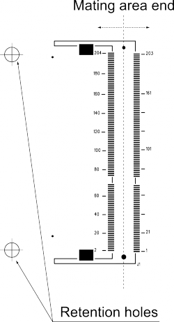
SO-DIMM mating connectors from different vendors may have slight differences in mechanical characteristics. One critical point is the position of the end of the mating area (please see the picture below), that can be slightly shifted inwards or outwards in respect to the retention holes on the carrier board. This can lead to a misalignment with the holes on the SO-DIMM modules, making difficult or impossible to insert the retentions screws or locking supports.
If you plan to use the holes as additional retention system, we recommend to pay attention to the mechanical characteristics when evaluating the SO-DIMM mating connectors to be mounted on the carrier board.
Power-up sequence[edit | edit source]
In order to prevent back powering effects, DAVE Embedded Systems' SOMs provide the signals required to handle power-up sequence properly. For instance, see the recommended sequence for the BORA SOM here.
In case the power-up sequence is not managed properly, the circuitry populating the SOM may be damaged.
Interfaces Guidelines[edit | edit source]
This section provides guidelines for the most used interfaces on DAVE Embedded Systems SOMs module.
Please refer to SOM's detailed pages for specific additional information.
Ethernet 10/100/1000[edit | edit source]
Case #1: PHY is integrated on SOM[edit | edit source]
This section refers to the case of PHY integrated on SOM such as Lizard and MAYA.
Schematics[edit | edit source]
- If LAN connector with integrated magnetic is used:
- predispose ethernet protection diodes on ethernet lines
- Connect connector shield to an adeguate GND or shield Plane
PCB[edit | edit source]
Refer to this table for 10/100 differential pairs routing
| Parameter for 10/100 differential pair | Min | Typ | Max |
| Differential Impedance(ohm) | - | 100 | - |
| Common Mode Impedance | - | 50 | - |
| Gap than TX and RX signals | 2xgap | 2xgap | - |
| Gap than other signals | 2xgap | 4xgap | - |
| Intra pair matching(mils)* | 0 | 25 | 150 |
| TX and RX via # mismatch* | 0 | 0 | 1 |
Refer to this table for Gigabit differential pairs routing
| Parameter for Gigabit Differential Pairs | Min | Typ | Max |
| Differential Impedance(ohm) | - | 100 | - |
| Common Mode Impedance | - | 50 | - |
| Gap than TX and RX signals | 2xgap | 2xgap | - |
| Gap than other signals | 2xgap | 4xgap | - |
| Intra pair matching(mils)* | 0 | 10 | 10 |
| Max PCB trace length | 3" | 5" | - |
| TX and RX via # mismatch* | 0 | 0 | 1 |
* Not mandatory but recommended.
- If LAN connector with integrated magnetic is used:
- do not route traces under the connettor, neither on opposite side
- place filter diode near connector
- place others signals far from connector
- Connect connector shield to an adeguate GND or shield Plane or Copper through numerous vias
- If on board magnetic are used
- adeguately isolate system GND from magnetic connector side
- Connect connector shield to an adeguate GND or shield Plane or Copper through numerous vias if necessary
- try to match as best as possible each differential pair (intrapair matching)
- Keep as best as possibile the same route for TX and RX traces
- If less than minimum gap is used, use a GND trace for improve trace separation
Case #2: PHY is not integrated on SOM and a RGMII PHY is used[edit | edit source]
This section refers to the case of:
- PHY not integrated on SOM
- Gigabit PHY populated on carrier board and connected to SOM through RGMII interface.
This solution is implemented on NaonEVB-Mid for example.
Schematics[edit | edit source]
- Add series resistors (RPACK resistors recommended) to RGMII lines
- Properly decouple PHY Power Supplies rails
- Properly decouple every supply pin of Ethernet PHY
- Properly separate analog Supply Rails
PCB[edit | edit source]
| Parameter for RGMII interface | Min | Typ | Max |
| Common mode impedance(ohm) | - | 50 | - |
| Gap than other ethernet diff pair | 4xwidth | - | - |
| Gap than other signals | 4xwidth | - | |
| Matching(mils) | - | - | 200 |
| Via Mismatch | 0 | 0 | 1 |
| Parameter for Gigabit Differential Pairs | Min | Typ | Max |
| Differential Impedance(ohm) | - | 100 | - |
| Common Mode Impedance | - | 50 | - |
| Gap than TX and RX signals | 2xgap | 2xgap | - |
| Gap than other signals | 2xgap | 4xgap | - |
| Intra pair matching(mils) | 0 | 10 | 10 |
| Max PCB trace length | 3" | 5" | - |
| TX and RX via # mismatch* | 0 | 0 | 1 |
* Not mandatory but recommended.
- Ground and VCC planes must be as large as possible
- Avoid plane split and voids
- Place bypass capacitor near every PHY supply pin
- Connect every capacitor's pin to the plane with at least 2 vias and the shortest trace pattern
- Place PHY device at least 1" (25mm) distance far away from connector
- Keep MDIO clock signal isolated from other signals
Case #3: PHY is not integrated on SOM and a RMII PHY is used[edit | edit source]
This section refers to the case of
- PHY not integrated on SOM
- 10/100 Ethernet PHY populate don carrier board and interfaced to SOM through RMII interface.
This solution is implemented for example in MayaEVB-Lite board.
Schematics[edit | edit source]
- If possible, place series resistor to RMII interface signals
- Properly decouple PHY Power Supplies rails
- Properly separate analog Supply Rails
- Properly decouple every supply pin of Ethernet PHY
- Use a standard RMII PHY that supports correct clock mode (see SOM specification for further details)
PCB[edit | edit source]
| Parameter for RMII interface | Min | Typ | Max |
| Reccomended Common mode impedance(ohm) | - | 50 | - |
| Gap between other signal | 2xW | - |
- Since RMII signals are not critical such as RGMII, is not necessary a strong matching between signal
- Avoid use of long traces
- Avoid stubs
- Keep as best as possibile the same routing for all RMII traces
| Parameter for Ethernet Differential Pairs | Min | Typ | Max |
| Differential Impedance(ohm) | - | 100 | - |
| Common Mode Impedance | - | 50 | - |
| Gap than other TX and RX signals | 2xgap | 2xgap | - |
| Gap than other signals | 2xgap | 4xgap | - |
| Intra pair matching(mils)* | 0 | 25 | 150 |
| TX and RX via # mismatch* | 0 | 0 | 1 |
* Not mandatory but recommended.
- Ground and VCC planes must be as large as possible
- Avoid plane split and voids
- Place bypass capacitor near every PHY supply pin
- Connect every capacitor's pin to the plane with at least 2 vias and the shortest trace pattern
- Place PHY device at least 1" (25mm) distance far away connector
- Keep MDIO clock signal isolated from other signals
USB[edit | edit source]
Schematics[edit | edit source]
- Create schematic in accordance with DAVE Embedded Systems system-on-modules (SOM) USB specification ( see SOM detailed pages )
PCB[edit | edit source]
| Parameter for USB Differential Pairs | Min | Typ | Max |
| Differential Impedance(ohm) | 80 | 90 | 100 |
| Common Mode Impedance | 40,5 | 45 | 49.5 |
| Gap than other signals | 3xgap | 5xgap | - |
| Intra pair matching(mils) | 0 | 25 | 150 |
| Max allowed stubs | - | - | 0 |
| Max traces length | - | - | note 1 |
| Max allowed plane split under traces | - | - | 0 |
note 1 see SOM detailed specifications
- If a stub is unavoidable in the design, no stub should be greater than 200 mils.
- Place a continuos reference plane underneath differential pair
HDMI[edit | edit source]
Schematics[edit | edit source]
- Add a Transmitter Port Protection to HDMI lines
- Use certified HDMI connector
- Connector shield must be properly connected
PCB[edit | edit source]
| Parameter for HDMI Differential Pairs | Min | Typ | Max |
| Differential Impedance(ohm) | 85 | 100 | 115 |
| Gap than other signals | 3xgap | 5xgap | - |
| Intra pair matching(mils) at 225MHz clock | 0 | 20 | 250 |
| Inter pair matching(mils) at 225MHz clock | 0 | 250 | 1" |
| Max allowed stubs | - | - | 0 |
| Max allowed plane split under traces | - | - | 0 |
- Place a continuos reference plane underneath differential pair
- Try to match lines as best as possible
SATA[edit | edit source]
Schematics[edit | edit source]
- Use certified SATA connector
PCB[edit | edit source]
| Parameter for SATA Differential Pairs | Min | Typ | Max |
| Differential Impedance(ohm) | 80 | 100 | 120 |
| Common Mode Impedance(ohm) | 51 | 60 | 69 |
| Gap than other signals | 2xgap | - | - |
| Intra pair matching(mils | - | - | note 1 |
| Inter pair matching(mils) | - | - | note 1 |
| Max allowed stubs | - | - | 0 |
| Max allowed plane split under traces | - | - | 0 |
| Max allowed length | - | - | note 1 |
note 1 see SOM detailed specifications
- Place a continuos reference plane underneath differential pair
- Minimized vias use
- No strong matching required between TX and RX, but keep same route for every differential pair
PCI Express[edit | edit source]
PCB[edit | edit source]
| Parameter for PCI Express Differential Pairs | Min | Typ | Max |
| Differential Impedance [Ohm] | - | 100 | - |
| Common Mode Impedance [Ohm] | - | 60 | - |
| Gap than other signals (reccomended) | - | 2xgap | - |
| Intra pair matching [mils]* | - | - | 10 |
| Max Total Length [in]* | - | - | 12 |
| Maximum allowed stub | - | - | 0 |
| Max allowed vias | - | - | 6 |
- * Including SoM trace length
- Preferred underneath plane over entire trace length GND.
LVDS[edit | edit source]
PCB[edit | edit source]
| Parameter for LVDS Differential Pairs | Min | Typ | Max |
| Differential Impedance [Ohm] | 85 | 100 | 115 |
| Common Mode Impedance [Ohm] | 46.75 | 55 | 63.25 |
| Gap than other signals (reccomended) | - | 2xgap | - |
| Intra pair skew [mils]* | - | - | 5 |
| Inter pair skew [mils]** | - | 400 | - |
| Maximum allowed stub | - | - | 0 |
- Prefer to route traces on TOP layer, referring them to a continuos GND plane.
- * Not includes SOM's length.
- ** Typical value can be relaxed depending on LVDS clock frequency
LCD Interface[edit | edit source]
Schematics[edit | edit source]
- Please refer to DAVE Embedded Systems system-on-modules (SOM) carrier board documentationfor further information
- Predispose series resistor terminator (RPACK for LCD data and single resistor for Clock and H-SYNC and V-SYNC)
- Series resistor value may vary depending by PCB and schematic
PCB[edit | edit source]
- If possible, use 50ohm common mode lines
- Match LCD parallel signals in accordance with Pixel Clock frequency (further details in SOM specifications)
- Avoid use of long traces connection (max 10" on PCB)
- Avoid stubs
VIN Interface[edit | edit source]
Schematics[edit | edit source]
- Please refer to DAVE Embedded Systems system-on-modules (SOM) carrier board documentation for further information
- Predispose series resistor terminator (RPACK for LCD data and single resistor for Clock and H-SYNC and V-SYNC)
- Series resistor value may vary depending PCB and schematic
PCB[edit | edit source]
- If possible, use 50ohm common mode lines
- Match VIN parallel signals in accordance with Pixel Clock frequency (further details in SOM specifications)
- Avoid use of long traces connection (max 10" on PCB)
- Avoid stubs
TVOUT[edit | edit source]
Schematics[edit | edit source]
- Please refer to DAVE Embedded Systems system-on-modules (SOM) carrier board documentation for further information
PCB[edit | edit source]
| Parameter for SATA Differential Pairs | Min | Typ | Max |
| Common Mode Impedance(ohm) | - | 75 | - |
| Gap than other signals | 2xwidth | - | - |
- Keep analog TVOUT signal far from noise signals
I2C Interface[edit | edit source]
Schematics[edit | edit source]
- Predispose properly pullup resistors on line in accordance with DAVE Embedded Systems system-on-modules (SOM)
- Do not overload I2C lines with too much devices
- Ensure that I2C devices are being properly initialized during power up
PCB[edit | edit source]
- Isolate I2C clock from noise sensitive signals
- Avoid stub
SD/MMC Interface[edit | edit source]
| Min | Typ | Max | |
| Common Mode impedance SOM(ohm) | - | 50 | 60 |
| Matching required* | - | - | - |
| Max allowed parallel routing(mils) | - | - | 1000 |
| Max trace Length** | - | - | - |
| Max # of vias allowed | - | - | - |
*This is not mandatory, however it is suggested in case trace length exceeds 10cm
**Overall trace length - i.e. Bora + carrier board - should not exceed 10cm. If this is not possible, try to avoid parallel routing in order to reduce crosstalk, and refer them to a ground plane.
CAN Interface[edit | edit source]
| Min | Typ | Max | |
| Differential Mode impedance(ohm) | 108 | 120 | 132 |
| Matching required | - | - | - |
| Min Interpair spacing | - | 4xgap | - |
| Max allowed parallel routing(mils) | - | - | - |
| Max trace Length | - | - | - |
| Max via allowed | - | - | - |
Functional guidelines[edit | edit source]
Sudden power off management[edit | edit source]
From the architectural standpoint, modern embedded systems often resemble traditional PCs. For example:
- they implement a rich set of I/O interfaces (large displays, Ethernet ports, USB ports, SDIO sockets etc.)
- they likely run complex operating systems that derive from desktop world (linux, Android, Windows CE etc.)
- they implement complex storage schemes (raw NAND, SSD, eMMC etc.).
One of the main difference between such systems and PCs is that the formers are - if appropriately designed - inherently resilient to sudden power fails. In any case, system designer should take into account these events and decide if and how manage them explicitly. Here are some typical techniques used to deal with this situation:
- in case the system is used by human operators, the use of clean shutdown - triggered by the user himself - should be encouraged to prevent sudden power off. Technically speaking, this can be done via GUI (soft button) or mechanical device (push buttons and alike). In the latter case, push button controllers such as Linear LTC2954 can be very useful to implement this feature
- in case no human operators interact with the system, more complex solutions might be required. This strategy is strongly dependent on hardware characteristics of SOM and must be approached on a case-by-case basis.
Thermal Management[edit | edit source]
Heat is generated by all semiconductors while operating and it is dissipated into the surrounding environment. This amount of heat is a function of the power consumed and the thermal resistance of the device package. Every silicon device on an electronic board must work within the limits of its operating temperature parameters (eg, the junction temperature) as specified by the silicon vendor.
Failure to maintain the temperature within safe ranges reduces operating lifetime, reliability, and performances and may cause irreversible damage to the system. Therefore, the product design cycle should include thermal analysis to verify that the device works within its functional limits. If the temperature is too high, component or system-level thermal enhancements are required to dissipate the heat from the system.
For detailed information, please refer to the following documents:
Interfaces and Connectors[edit | edit source]
Power Supply interface[edit | edit source]
The Evaluation Kit is powered by one of the USB Type-C connectors. To properly power the system the wall adapter must support the power delivery protocol.
Description[edit | edit source]
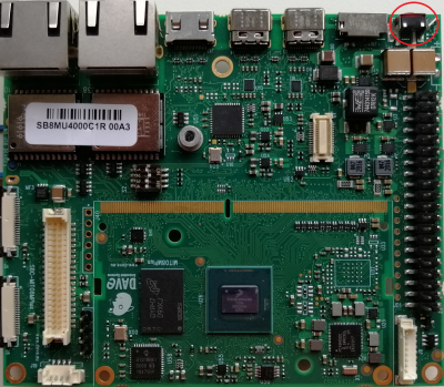
The Power Supply interface available on the Evaluation Kit at the connector J3
J3 is a USB Type-C connector for USB3 data transfer and board supply,
Signals[edit | edit source]
The following table describes the interface signals:
| Pin# | Pin name | Pin function | Pin Notes |
|---|---|---|---|
| A4, A9, B4, B9 | VBUS1 | Board supply | |
| A1, A12, B1, B12 | GND | Ground | |
| A6, A7, B6, B7, A2, A3, B10, B11, B2, B3, A10, A11, A5, B5, A8, B8 | USB signals | See USB ports |
Power LED[edit | edit source]
DL2 is a green LED (placed near the reset button) that shows the status of the power input. This LED is ON when a valid power supply is present and the system is out of reset.
Device usage[edit | edit source]
The USB-C PD protocol starts providing 5V to the system, this voltage is enough to boot the CPU and execute the bootloader.
The bootloader starts the PD handshake with the wall adapter and chose the input rail voltage between 5V, 9V, 12V, 15V or 20V.
By default the Evaluation Kit sets the input to 12V for LCD backlight compatibility, see the LVDS section for more details.
Alternate supply[edit | edit source]
An auxiliary connector is present on the board (not mounted by default) to power the system with a standard power supply.
This connector is meant for developing purpose (eg when the SW is not already able to handshake a valid PD profile) and cannot be mounted for some Evaluation Kit models.
Description[edit | edit source]
Power can be provided through the J20 connector. Power voltage range is +[12-24 V].
J20 is a two pins MC 1,5/2-G-3,81 Phoenix connector.
Signals[edit | edit source]
The following table describes the interface signals:
| Pin# | Pin name | Pin function | Voltage range | Notes |
|---|---|---|---|---|
| 1 | VIN_AUX | Board supply | +[12-24 V] | VIN_AUX is connected to J40 backlight connector and J20 pin 24 for LCD panel backlight power supply |
| 2 | GND | Ground |
CPU connector[edit | edit source]
J15 is the 260-pins SODIMM connector of the ORCA SOM.
In this SBC design the SOM is embedded in the carrier board so the connector is not actually usable but represents the SOM J1 connector.
For a detailed description of the SOM pinout, please refer to the ORCA SOM Hardware Manual.
JTAG interface[edit | edit source]
JTAG interface allow the developer to access every peripheral of the SoC using a debugger.
It is also possible to add the ETH1 PHY to the JTAG daisy chain (with a custom BOM).
The TRACE interface can be made available in alternative to the NAND or eMMC memory flash on board of the SoM.
Description[edit | edit source]
The JTAG interface available on the Evaluation Kit at the connector JD1.
JD1 is a 10x1x2.54mm strip header connector and it is not mounted.
Signals[edit | edit source]
The following table describes the interface signals:
| Pin# | Pin name | Function | ARM-20 JTAG | Notes |
|---|---|---|---|---|
| 1 | DGND | - | 4,6,8,10,12,14,16,18,20 | For example documented on Lauterbach specification |
| 2 | JTAG_TCK | - | 9 | - |
| 3 | JTAG_TMS | - | 7 | - |
| 4 | JTAG_TDO | - | 13 | - |
| 5 | JTAG_TDI | - | 5 | - |
| 6 | JTAG_MOD | - | - | 10K pull-down inside the SoM |
| 7 | CPU_PORn | - | 15 (*) | - |
| 8 | N.C. | - | - | - |
| 9 | N.C. | - | - | - |
| 10 | JTAG_VREF | - | 1 | 3V3 (BOARD_PGOOD driven signal) |
(*) optional signals, keep the possibility to be unconnected.
Ethernet interfaces[edit | edit source]
The Evaluation Kit features two Gigabit Ethernet interfaces:
- ETH0 on J10 (on schematics)
- this interface also features the TSN functionality
- ETH1 on J38 (on schematics)
Description[edit | edit source]
The Ethernet interfaces are available on the Evaluation Kit at the connectors J10 and J38.
J10 and J38 are RJ45 shielded connectors with dual leds. J10 is connected to the SoM's ethernet PHY, J38 is connected to the carrier's ethernet PHY
Signals[edit | edit source]
The following table describes the interfaces signals:
- J10
| Pin# | Pin name | Pin Notes |
|---|---|---|
| 1 | ETH0_TXRX1_P | |
| 2 | ETH0_TXRX1_N | |
| 3 | ETH0_TXRX2_P | |
| 4 | ETH0_TXRX3_P | |
| 5 | ETH0_TXRX3_N | |
| 6 | ETH0_TXRX2_N | |
| 7 | ETH0_TXRX4_P | |
| 8 | ETH0_TXRX4_N | |
| 9 | ETH0_LED_ACT | ETH0 has active low signals |
| 11 | ETH0_LED_LINK | ETH0 has active low signals |
- J38
| Pin# | Pin name | Pin Notes |
|---|---|---|
| 1 | ETH1_TXRX1_P | |
| 2 | ETH1_TXRX1_N | |
| 3 | ETH1_TXRX2_P | |
| 4 | ETH1_TXRX3_P | |
| 5 | ETH1_TXRX3_N | |
| 6 | ETH1_TXRX2_N | |
| 7 | ETH1_TXRX4_P | |
| 8 | ETH1_TXRX4_N | |
| 10 | ETH1_LED_ACT | ETH1 has active high signals |
| 12 | ETH1_LED_LINK | ETH1 has active high signals |
Device mapping[edit | edit source]
|
The ethernet names in the schematics (
|
eth0 (on J38) is the default network interface used by the Linux root file system and configured as primary interface.
Device usage[edit | edit source]
The peripherals use the standard kernel interface and network protocol stack.
Console interface[edit | edit source]
Description[edit | edit source]
The Console interface is available on the Evaluation Kit at the connector J35.
J35 is a 4 pin (4x1x2.54mm) header connector for the two-wires UART2 port, used for debug purposes (bootloader and operating system serial console).
Signals[edit | edit source]
The following table describes the interface signals:
| Pin# | SOM Pin# | Pin name | Pin function | Pin Notes |
|---|---|---|---|---|
| 1 | J15.250 | UART2_TXD | Transmit line | |
| 2 | J15.248 | UART2_RXD | Receive line | 10K pull-up to 3V3_CB |
| 3 | - | 3V3_CB | Power output for transceiver supply | BOARD_PGOOD driven rail |
| 4 | - | DGND | Ground |
Device mapping[edit | edit source]
UART2 is mapped to /dev/ttymxc1 device in Linux. The peripheral is used as the default serial console, both for the bootloader and the kernel.
Device usage[edit | edit source]
To connect to the debug serial port:
- connect an UART transceiver (eg: TTL-232RGVIP-WE) to J35 and to a workstation
- leave J35.3 unconnected if the transceiver is self powered
- start your favorite terminal emulator software on PC (eg: PuTTY); communication parameters are: 115200,8N1
UARTs interface[edit | edit source]
Description[edit | edit source]
The UARTs interfaces available on the Evaluation Kit are mapped to the following connectors:
- J8 is a 20x2x2.54mm pin header expansion connector that delivers many interfaces unused on board. On this connector are mapped these instances: UART1; UART2 (default debug console); UART4.
- J9 is a 8x1x1.25mm 53398-0871 Molex connector that delivers one RS232 4 wires (mapped to UART1) and one RS485 2 wires (mapped to UART3)
Signals[edit | edit source]
The following tables describe the interfaces signals:
J8[edit | edit source]
| Pin# | SOM Pin# | Pin name | Pin function | Pin Notes |
|---|---|---|---|---|
| 7 | J15.150 | SAI2_TXFS | UART1_CTS | shared with RS232 |
| 8 | J15.144 | SAI2_RXFS | UART1_TXD | shared with RS232 |
| 10 | J15.140 | SAI2_RXC | UART1_RXD | shared with RS232 |
| 11 | J15.142 | SAI2_RXD0 | UART1_RTS | shared with RS232 |
| 19 | J15.122 | ECSPI2_MOSI | UART4_TXD | Transmit signal (OUT) |
| 21 | J15.120 | ECSPI2_MISO | UART4_CTS | Clear to send (OUT) |
| 23 | J15.124 | ECSPI2_SCLK | UART4_RXD | Receive signal (IN) |
| 24 | J15.126 | ECSPI2_SS0 | UART4_RTS | Request to send (IN) |
| 27 | J15.248 | UART2_RXD | UART2_RXD | default debug console |
| 29 | J15.250 | UART2_TXD | UART2_TXD | default debug console |
| 31 | J15.256 | UART4_RXD | UART4_RXD | alternative to ECSPI2_SCLK |
| 33 | J15.258 | UART4_TXD | UART4_TXD | alternative to ECSPI2_MOSI |
| 1, 17 | - | 3V3_CB | Power output for transceiver supply | BOARD_PGOOD driven rail |
| 6, 9, 14, 20, 25, 30, 34, 39 | - | DGND | Ground |
J9[edit | edit source]
| Pin# | SOM Pin# | Pin name | Pin function | Pin Notes |
|---|---|---|---|---|
| 1 | - | RS485_A | Non inverting BUS signal | UART3 |
| 2 | - | RS485_B | Inverting BUS signal | UART3 |
| 3 | - | RS485_B_120R | Termination resistor | connect this signal to RS485_B
to enable the 120R termination |
| 4 | - | DGND | Ground | |
| 5 | J15.144 | RS232_TX | Transmit line | UART1_TXD (shared with J8.8) |
| 6 | J15.140 | RS232_RX | Receive line | UART1_RXD (shared with J8.10) |
| 7 | J15.150 | RS232_CTS | Clear to send line | UART1_CTS (shared with J8.7) |
| 8 | J15.142 | RS232_RTS | Request to send line | UART1_RTS (shared with J8.11) |
Device mapping[edit | edit source]
UART1 is mapped to /dev/ttymxc0 device in Linux
UART2 is mapped to /dev/ttymxc1 device in Linux. The peripheral is used as the default serial console, both for the bootloader and the kernel.
UART3 is mapped to /dev/ttymxc2 device in Linux
UART4 is mapped to /dev/ttymxc3 device in Linux
Device usage[edit | edit source]
The TTL UARTs on J8 can be connected to external devices that use 0-3.3V levels.
The RS232 and RS485 uses the standard protocols.
micro SD interface[edit | edit source]
Description[edit | edit source]
The micro SD interface available on the Evaluation Kit at the connector J16, labelled as uSD on the bottom.
J16 is a Micro-SD card header. This interface is connected to the USDHC2 controller of the i.MX8M Plus CPU.
Signals[edit | edit source]
The following table describes the interface signals:
| Pin# | SOM Pin# | Pin name | Pin function | Pin Notes |
|---|---|---|---|---|
| 1 | J15.52 | SD_DAT2 | Data 2 | |
| 2 | J15.54 | SD_DAT3 | Data 3 | |
| 3 | J15.46 | SD_CMD | CMD | |
| 4 | - | VDD | +3.3 V | BOARD_PGOOD driven rail with 200mA fuse |
| 5 | J15.44 | SD_CLK | Clock | |
| 6, 12 | - | VSS | Ground | |
| 7 | J15.48 | SD_DAT0 | Data 0 | |
| 8 | J15.50 | SD_DAT1 | Data 1 | |
| 9, 10, 11 | - | SD_SHIELD | Shield | |
| 13 | J15.42 | SD2_CD_B | Card detect |
Device mapping[edit | edit source]
The microSD card is mapped to /dev/mmcblk1. The available partitions are shown as /dev/mmcblk1p1, /dev/mmcblk1p2, etc.
Device usage[edit | edit source]
The device can be mounted/accessed as a standard block device in Linux.
USB Ports interface[edit | edit source]
Description[edit | edit source]
The Evaluation Kit provides two USB3.0 ports at the connectors J3 and J4.
J3 and J4 are USB Type-C connectors. J3(right side on the image) is also used to supply the system, see Power Supply section.
Both ports can provide 5V output up to 2.2A. J3 port can also be configured to provide up to 3.3A
Signals[edit | edit source]
The following table describes the interfaces signals:
J3[edit | edit source]
| Pin# | SOM Pin# | Pin name | Pin function | Pin Notes |
|---|---|---|---|---|
| A4, A9, B4, B9 | - | VBUS | +5V | |
| A6, B6 | J15.193 | DP1 | USB_DP | |
| A7, B7 | J15.195 | DN1 | USB_DN | |
| A2 | J15.199 | SSTXP1 | USB_TX_P | |
| A3 | J15.201 | SSTXN1 | USB_TX_N | |
| B11 | J15.203 | SSRXP1 | USB_RX_P | |
| B10 | J15.205 | SSRXN1 | USB_RX_N | |
| B2 | J15.199 | SSTXP2 | USB_TX_P | |
| B3 | J15.201 | SSTXN2 | USB_TX_N | |
| A11 | J15.203 | SSRXP2 | USB_RX_P | |
| A10 | J15.205 | SSRXN2 | USB_RX_N | |
| A5 | - | CC1 | Orientation Plug | Used for PD handshake |
| B5 | - | CC2 | Orientation Plug | Used for PD handshake |
| A8 | - | SBU1 | Side Band Use | |
| B8 | - | SBU2 | Side Band Use | |
| A1, A12, B1, B12 | - | DGND | Ground |
J4[edit | edit source]
| Pin# | SOM Pin# | Pin name | Pin function |
|---|---|---|---|
| A4, A9, B4, B9 | - | VBUS | +5V |
| A6, B6 | J15.173 | DP1 | USB_DP |
| A7, B7 | J15.175 | DN1 | USB_DN |
| A2 | J15.179 | SSTXP1 | USB_TX_P |
| A3 | J15.181 | SSTXN1 | USB_TX_N |
| B11 | J15.183 | SSRXP1 | USB_RX_P |
| B10 | J15.185 | SSRXN1 | USB_RX_N |
| B2 | J15.179 | SSTXP2 | USB_TX_P |
| B3 | J15.181 | SSTXN2 | USB_TX_N |
| A11 | J15.183 | SSRXP2 | USB_RX_P |
| A10 | J15.185 | SSRXN2 | USB_RX_N |
| A5 | - | CC1 | Orientation Plug |
| B5 | - | CC2 | Orientation Plug |
| A8 | - | SBU1 | Side Band Use |
| B8 | - | SBU2 | Side Band Use |
| A1, A12, B1, B12 | - | DGND | Ground |
Device usage[edit | edit source]
The USB ports can be used under Linux for connecting USB devices: the related device driver has to be integrated into the Linux kernel.
To connect USB devices to J3 an USB-C HUB has to be used for power the Evaluation Kit while transferring USB data. Please check that the chosen HUB is qualified for the Power Delivery protocol.
LVDS interface[edit | edit source]
Description[edit | edit source]
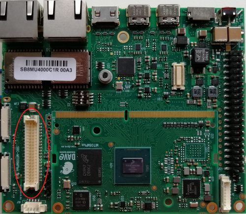
The LVDS interface available on the Evaluation Kit at the connector J13
J13 is a 20x2x1.25mm DF13E-40DP-1.25V(51) Hirose header connector.
On this connector are routed two separate LVDS interfaces that can operate in dual-channel mode to drive high resolution displays.
Signals[edit | edit source]
The following table describes the interfaces signals:
| Pin# | SOM Pin# | Pin name | Pin function | Pin Notes |
|---|---|---|---|---|
| 1, 3 | - | 3V3_LCD | Power output | GPIO driven rail |
| 7 | J15.49 | LVDS0_D0_N | LVDS Data 0 - | |
| 9 | J15.51 | LVDS0_D0_P | LVDS Data 0 + | |
| 2 | J15.45 | LVDS0_D1_N | LVDS Data 1 - | |
| 4 | J15.47 | LVDS0_D1_P | LVDS Data 1 + | |
| 13 | J15.37 | LVDS0_D2_N | LVDS Data 2 - | |
| 15 | J15.39 | LVDS0_D2_P | LVDS Data 2 + | |
| 19 | J15.41 | LVDS0_CLK_N | LVDS Clock - | |
| 21 | J15.43 | LVDS0_CLK_P | LVDS Clock + | |
| 8 | J15.33 | LVDS0_D3_N | LVDS Data 3 - | |
| 10 | J15.35 | LVDS0_D3_P | LVDS Data 3 + | |
| 5, 6, 11, 12, 17, 18, 23, 26, 29, 32, 35 | - | DGND | Ground | |
| 25 | J15.71 | LVDS1_D0_N | LVDS Data 0 - | |
| 27 | J15.73 | LVDS1_D0_P | LVDS Data 0 + | |
| 31 | J15.67 | LVDS1_D1_N | LVDS Data 1 - | |
| 33 | J15.69 | LVDS1_D1_P | LVDS Data 1 + | |
| 28 | J15.59 | LVDS1_D2_N | LVDS Data 2 - | |
| 30 | J15.61 | LVDS1_D2_P | LVDS Data 2 + | |
| 34 | J15.63 | LVDS1_CLK_N | LVDS Clock - | Can be terminated on board
for dual-channel mode |
| 36 | J15.65 | LVDS1_CLK_P | LVDS Clock + | |
| 37 | J15.55 | LVDS1_D3_N | LVDS Data 3 - | |
| 39 | J15.57 | LVDS1_D3_P | LVDS Data 3 + | |
| 14, 16, 18 | - | 5V_LCD | Power output | GPIO driven rail |
| 20 | - | VIN_BL_AUX1 | Power output | Default connected to VIN_BL.
Can be connected to an external controller to generate custom rails. |
| 22 | - | VIN_BL_AUX2 | Power output | |
| 24 | - | VIN_BL | Power output | GPIO driven rail |
| 38 | J15.240 | LCD_BKLT_PWM | PWM output | Default routed to PWM1
Can be routed to PWM2 |
| 40 | J15.213 | LCD_EN | GPIO |
Device mapping[edit | edit source]
- LVDS0 is typically mapped to
/dev/fb0device in Linux - LVDS1 is mapped to the corresponding device driver in Linux, depending on the
ldbperipheral configuration in the device tree. The default value is disabled but can be mapped to/dev/fb2(second and independent LCD panel) or can be the second LVDS channel for a dual-channel LCD panel configuration (like a 1920x1080 DUAL LVDS channel LCD panel)
Power sequence[edit | edit source]
Most of the LCD panels has many supplies and need a specific timing to power the rails and start the the signals.
The Evaluation Kit provides GPIO controlled power rails that can be leveraged both at bootloader and kernel level to meet any specifications.
The following sections describe the available rails:
3V3_LCD[edit | edit source]
The most common voltage to supply the LCD panel internal logic. This rail is enabled by GPIO1_IO06 that is connected to J15.233
5V_LCD[edit | edit source]
The most common voltage to supply the LCD panel backlight. This rail is enabled by GPIO1_IO08 that is connected to J15.209
VIN_LCD[edit | edit source]
The voltage of this rail is the system input voltage, see Power Supply section for more details. This rail is enabled by GPIO1_IO07 that is connected to J15.225
VIN_LCD_AUX[edit | edit source]
There are two more pins to deliver higher current on the rail VIN_LCD. These two pins can be instead separately routed to the expansion connector J40.
J40 is a 6x1x2.54mm strip header connector, not mounted by default. This connector can house an external controller that generates up to 2 custom rails, controlled by GPIOs.
J40 Signals[edit | edit source]
The following table describes the interface signals:
| Pin# | SOM Pin# | Pin name | Pin function | Pin Notes |
|---|---|---|---|---|
| 1 | - | VIN | Power output | This is the input power supply voltage |
| 2 | J15.240 | LCD_BKLT_PWM | PWM output | Default routed to PWM1
Can be routed to PWM2 |
| 3 | J15.225 | GPIO1_IO07 | GPIO | |
| 4 | - | VIN_BL_AUX2 | Power input | Alternative external backlight power supply |
| 5 | - | VIN_BL_AUX1 | Power input | Alternative external backlight power supply |
| 6 | - | DGND | Ground |
Device usage[edit | edit source]
The display power sequence can be leveraged by a DAVE custom code that allow to set the timings both in U-boot and in Linux kernel sources.
The associated framebuffer device is accessed in Linux through the standard graphic access.
Touchscreen interface[edit | edit source]
Description[edit | edit source]
The Evaluation Kit default LCD panel (provided on request) interfaces the touchscreen via USB, thus it is connected to J3 or J4, see USB ports section.
Many touchscreen types use instead an I2C interface with two additional control signals (RST, IRQ).
To use these type of touchscreens the interface signals can be routed to the expansion connector J8.
An external circuit is recommended to correctly conditioning the interface signals, such as buffers and pull up/down, according to the touchscreen specifications.
Signals[edit | edit source]
The following table describes the available I2C signals on J8 connector, see GPIO section for available control signals:
| Pin# | SOM Pin# | Pin name | Pin function | Pin Notes |
|---|---|---|---|---|
| 19 | ECSPI2_MOSI | I2C3_SDA | ||
| 21 | ECSPI2_MISO | I2C4_SCL | ||
| 22 | SAI5_MCLK | I2C5_SDA | ||
| 23 | ECSPI2_SCLK | I2C3_SCL | ||
| 24 | ECSPI2_SS0 | I2C4_SDA | ||
| 32 | SAI5_RXFS | I2C6_SCL | ||
| 38 | SAI5_RXD0 | I2C5_SCL | ||
| 40 | SAI5_RXC | I2C6_SDA | ||
| 1, 17 | - | 3V3_CB | +3.3V | BOARD_PGOOD driven rail |
| 2, 4 | - | 5V_VIN | +5V | Always powered |
| 6, 9, 14, 20, 25, 30, 34, 39 | - | DGND | Ground |
All the I2C signals use 0 - 3.3V levels, external pull-ups to 3V3_CB are needed.
Device mapping[edit | edit source]
The device is typically mapped to /dev/touchscreen0 device in Linux.
The touch controller is attached to the generic Linux input event interface (evdev).
For I2C touchscreen controllers a dedicated node in the device-tree has to be configured to correctly bind the driver.
Device usage[edit | edit source]
The touchscreen device is often passed as parameter to the user interface application or is automatically discovered.
Touchscreen can be tested with the evtest tool that prints the finger coordinates to the console.
HDMI interface[edit | edit source]
Description[edit | edit source]
The HDMI interface available on the Evaluation Kit at the connector J12, labelled as HDMI on the bottom.
J12 is a Mini HDMI horizontal receptacle connector.
Signals[edit | edit source]
The following table describes the interface signals:
| Pin# | SOM Pin# | Pin name | Pin function | Pin Notes |
|---|---|---|---|---|
| 2 | J15.98 | HDMI_D2P | TX pair 2 data + | |
| 3 | J15.96 | HDMI_D2N | TX pair 2 data - | |
| 5 | J15.94 | HDMI_D1P | TX pair 1 data + | |
| 6 | J15.92 | HDMI_D1N | TX pair 1 data - | |
| 8 | J15.90 | HDMI_D0P | TX pair 0 data + | |
| 9 | J15.88 | HDMI_D0N | TX pair 0 data - | |
| 11 | J15.86 | HDMI_CLKP | Tx pair clock + | |
| 12 | J15.84 | HDMI_CLKN | Tx pair clock - | |
| 14 | J15.74 | CEC | Consumer Electric Control | |
| 15 | J15.76 | SCL | I2C clock | |
| 16 | J15.78 | SDA | I2C data | |
| 18 | - | 5V | +5V power output | Internal 200mA fuse |
| 19 | J15.80/J15.104 | HPD/HEAC- | Hotplug detection / ARC-HEC | |
| 1, 4, 7, 10, 13 | - | DGND | Ground | |
| 17 | J15.102 | HEAC+ | HDMI Ethernet Audio Return Channel |
Device mapping[edit | edit source]
HDMI video is mapped to the corresponding device driver in Linux, depending on the device tree configuration. If this is the only video output, then the default value is mapped to /dev/fb0.
Device usage[edit | edit source]
The associated framebuffer device is accessed in Linux through the standard graphic access.
MIPI interface[edit | edit source]
There are two MIPI camera inputs and one MIPI display output available on the Evaluation Kit.
Description[edit | edit source]
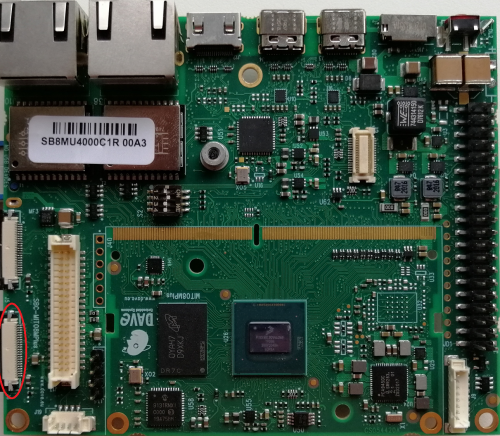
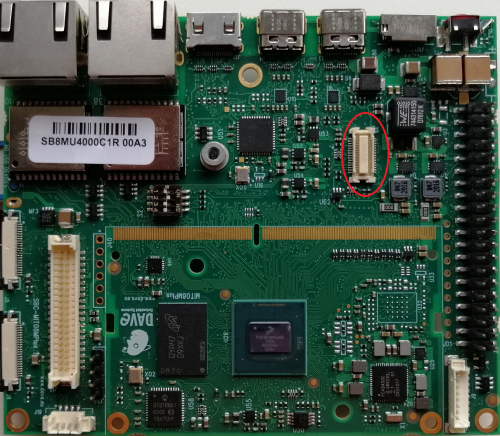
The MIPI camera interfaces are available on the Evaluation Kit at the connectors J5 and J6.
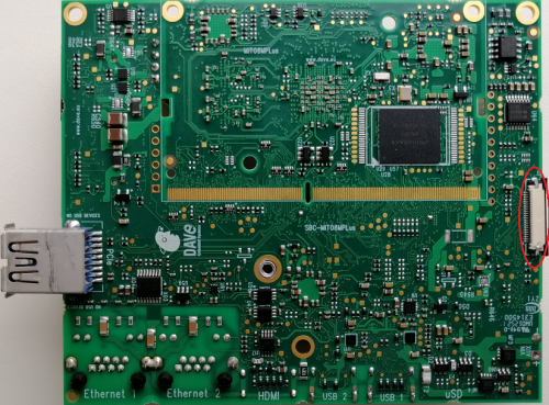
The MIPI display interface is available on the Evaluation Kit at the connector J7 (and it is located at the bottom side of ORCA SBC)
J5, J6 and J7 are a 22x1x0.5mm horizontal ZIF connectors that deliver the MIPI signals, many control signals and power.
Signals[edit | edit source]
The following tables describe the interfaces signals:
J5[edit | edit source]
| Pin# | SOM Pin# | Pin name | Pin function | Pin Notes |
|---|---|---|---|---|
| 1, 4, 7, 10, 13 | - | DGND | Ground | |
| 2 | J15.117 | MIPI_CSI1_D0_N | MIPI Data 0 - | |
| 3 | J15.115 | MIPI_CSI1_D0_P | MIPI Data 0 + | |
| 5 | J15.113 | MIPI_CSI1_D1_N | MIPI Data 1 - | |
| 6 | J15.111 | MIPI_CSI1_D1_P | MIPI Data 1 + | |
| 8 | J15.109 | MIPI_CSI1_CLK_N | MIPI Clock - | |
| 9 | J15.107 | MIPI_CSI1_CLK_P | MIPI Clock + | |
| 11 | J15.105 | MIPI_CSI1_D2_N | MIPI Data 2 - | |
| 12 | J15.103 | MIPI_CSI1_D2_P | MIPI Data 2 + | |
| 14 | J15.101 | MIPI_CSI1_D3_N | MIPI Data 3 - | |
| 15 | J15.99 | MIPI_CSI1_D3_P | MIPI Data 3 + | |
| 16 | - | CAM1_IO2/GND | CSI_nRST/Ground | Default connected to Ground
Can be alternatively routed to J15.233 GPIO |
| 17 | J15.227 | CAM1_IO0 | CSI_MCLK | |
| 18 | J15.231 | CAM1_IO1 | CSI1_SYNC | |
| 19 | - | CAM1_IO3/GND | CSI_MCLK/Ground | Default connected to Ground
Can be alternatively routed to J15.38 GPIO |
| 20 | J15.230 | CAM1_SCL | I2C2_SCL | 4K7 internal pull-up |
| 21 | J15.232 | CAM1_SDA | I2C2_SDA | 4K7 internal pull-up |
| 22 | - | MIPI_CSI1_PSU | +3.3V | Default connected to 3V3_CB
Can be alternatively routed to 5V_CB or VIN |
J6[edit | edit source]
| Pin# | SOM Pin# | Pin name | Pin function | Pin Notes |
|---|---|---|---|---|
| 1, 4, 7, 10, 13 | - | DGND | Ground | |
| 2 | J15.79 | MIPI_CSI2_D0_N | MIPI Data 0 - | |
| 3 | J15.77 | MIPI_CSI2_D0_P | MIPI Data 0 + | |
| 5 | J15.83 | MIPI_CSI2_D1_N | MIPI Data 1 - | |
| 6 | J15.81 | MIPI_CSI2_D1_P | MIPI Data 1 + | |
| 8 | J15.87 | MIPI_CSI2_CLK_N | MIPI Clock - | |
| 9 | J15.85 | MIPI_CSI2_CLK_P | MIPI Clock + | |
| 11 | J15.91 | MIPI_CSI2_D2_N | MIPI Data 2 - | |
| 12 | J15.89 | MIPI_CSI2_D2_P | MIPI Data 2 + | |
| 14 | J15.95 | MIPI_CSI2_D3_N | MIPI Data 3 - | |
| 15 | J15.93 | MIPI_CSI2_D3_P | MIPI Data 3 + | |
| 16 | - | CAM2_IO2/GND | CSI_nRST/Ground | Default connected to Ground
Can be alternatively routed to J15.233 GPIO |
| 17 | J15.227 | CAM2_IO0 | CSI_MCLK | |
| 18 | J15.225 | CAM2_IO1 | CSI2_SYNC | |
| 19 | - | CAM2_IO3/GND | CSI_MCLK/Ground | Default connected to Ground
Can be alternatively routed to J15.38 GPIO |
| 20 | J15.234 | CAM2_SCL | I2C3_SCL | 4K7 internal pull-up |
| 21 | J15.236 | CAM2_SDA | I2C3_SDA | 4K7 internal pull-up |
| 22 | - | MIPI_CSI1_PSU | Power supply | Default connected to 3V3_CB
Can be alternatively routed to 5V_CB or VIN |
J7[edit | edit source]
| Pin# | SOM Pin# | Pin name | Pin function | Pin Notes |
|---|---|---|---|---|
| 1, 4, 7, 10, 13, 20 | - | DGND | Ground | |
| 2 | J15.135 | MIPI_DSI1_D1_N | MIPI Data 1 - | |
| 3 | J15.133 | MIPI_DSI1_D1_P | MIPI Data 1 + | |
| 5 | J15.131 | MIPI_DSI1_CLK_N | MIPI Clock - | |
| 6 | J15.129 | MIPI_DSI1_CLK_P | MIPI Clock + | |
| 8 | J15.139 | MIPI_DSI1_D0_N | MIPI Data 0 - | |
| 9 | J15.137 | MIPI_DSI1_D0_P | MIPI Data 0 + | |
| 11 | J15.127 | MIPI_DSI1_D2_N | MIPI Data 2 - | |
| 12 | J15.125 | MIPI_DSI1_D2_P | MIPI Data 2 + | |
| 14 | J15.123 | MIPI_DSI1_D3_N | MIPI Data 3 - | |
| 15 | J15.121 | MIPI_DSI1_D3_P | MIPI Data 3 + | |
| 16 | J15.209 | DSI_EN | GPIO | |
| 17 | J15.230 | DISP1_SCL | I2C2_SCL | 4K7 internal pull-up |
| 18 | J15.232 | DISP1_SDA | I2C2_SDA | 4K7 internal pull-up |
| 19 | J15.217 | DSI_BL_PWM | PWM/GPIO | Can be alternatively routed to Ground |
| 21, 22 | - | MIPI_CSI1_PSU | Power supply | Default connected to 3V3_CB
Can be alternatively routed to 5V_CB |
Device mapping[edit | edit source]
The MIPI CSI peripherals are mapped to the corresponding /dev/video<X> device in Linux.
The MIPI DSI peripherals are mapped to the corresponding /dev/fb<X> device in Linux.
The devices mapping depends on the device tree configuration.
Device usage[edit | edit source]
The devices are accessed in Linux through the standard graphic stack.
PCIe interface[edit | edit source]
Description[edit | edit source]
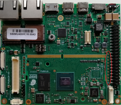
The PCI Express interface can be available on the Evaluation Kit at the connector J36. This connector is not mounted by default.
J36 is a USB3.0 Type-A connector that delivers 1x PCIe slot. An external adapter is needed to route the signals to a standard PCIe connector.
The external adapter can be found as a PCIe riser, commonly used in Ethereum mining like this one.
|
WARNING: do not connect USB devices to this port! |
Signals[edit | edit source]
The following table describes the interface signals:
| Pin# | SOM Pin# | Pin name | Pin function | Pin Notes |
|---|---|---|---|---|
| 1 | - | VBUS | PCIE_WAKE# | Routed to a test point |
| 2 | J15.157 | D- | PCIE2_REF_CN_CLKN | |
| 3 | J15.155 | D+ | PCIE2_REF_CN_CLKP | |
| 4 | - | GND | PCIE_PERST# | Routed to a test point |
| 5 | J15.159 | SSRX- | PCIE_TXN_P | Internally decoupled with 100nF series |
| 6 | J15.161 | SSRX+ | PCIE_TXN_N | Internally decoupled with 100nF series |
| 7 | - | GND_D | Ground | |
| 8 | J15.163 | SSTX- | PCIE_RXN_P | |
| 9 | J15.165 | SSTX+ | PCIE_RXN_N |
Device mapping[edit | edit source]
The PCI express peripheral is mapped to the corresponding device in Linux depending on the associated kernel device driver and on the device tree configuration.
CAN interface[edit | edit source]
Description[edit | edit source]
The CAN interfaces are available on the Evaluation Kit at the connector J8.
J8 is a 20x2x2.54mm pin header expansion connector that delivers many interfaces unused on board and can provide up to two CAN ports.
The CAN bus ports are compatible with the Flexible Data rate (CAN FD) and CAN 2.0B protocols specification.
Signals[edit | edit source]
The following table describes the interface signals:
| Pin# | SOM Pin# | Pin name | Pin function | Pin Notes |
|---|---|---|---|---|
| 10 | J15.140 | SAI2_RXC | CAN1_TX | |
| 12 | J15.146 | SAI2_TXC | CAN1_RX | |
| 16 | J15.148 | SAI2_TXD0 | CAN2_TX | |
| 18 | J15.138 | SAI2_MCLK | CAN2_RX | |
| 22 | J15.166 | SAI5_MCLK | CAN2_RX | |
| 35 | J15.176 | SAI5_RXD3 | CAN2_TX | |
| 36 | J15.174 | SAI5_RXD2 | CAN1_RX | |
| 37 | J15.172 | SAI5_RXD1 | CAN1_TX | |
| 2, 4 | - | 5V_VIN | Power output for transceiver supply | Always ON rail |
| 1, 17 | - | 3V3_CB | Power output for transceiver supply | BOARD_PGOOD driven rail |
| 6, 9, 14, 20, 25, 30, 34, 39 | - | DGND | Ground |
Please note that all the CAN signals are 0-3.3V level. If a 5V powered transceiver is used, a level shifting is needed to interface to the Evaluation Kit connector.
Device mapping[edit | edit source]
CAN devices are mapped to /dev/can<X> device in Linux. The device mapping depends on the device tree configuration.
Device usage[edit | edit source]
The Evaluation Kit doesn't implement any CAN transceiver, these are needed to mediate between the CAN bus and the CPU module.
The peripheral can be configured using ifconfig and ip link utilities and can be tested with the can-utils utilities.
Audio interface[edit | edit source]
There is no directly available Audio interface on the Evaluation Kit, two SAI and one SPDIF full duplex interfaces are available on the expansion connector.
Description[edit | edit source]
The SAI and SPDIF interfaces are available on the Evaluation Kit at the connector J8.
J8 is a 20x2x2.54mm pin header expansion connector that delivers many interfaces unused on board.
Signals[edit | edit source]
The following table describes the interfaces signals:
| Pin# | SOM Pin# | Pin name | Pin function | Pin Notes |
|---|---|---|---|---|
| 1, 17 | - | 3V3_CB | Power output for transceiver supply | BOARD_PGOOD driven rail |
| 2, 4 | - | 5V_VIN | Power output for transceiver supply | Always ON rail |
| 6, 9, 14, 20,
25, 30, 34, 39 |
- | DGND | Ground | |
| 7 | J15. | SAI2_TXFS | Transmit Frame Sync | |
| 8 | J15. | SAI2_RXFS | Receive Frame Sync | |
| 10 | J15. | SAI2_RXC | Receive Bit Clock | |
| 11 | J15. | SAI2_RXD0 | Receive Data 0 | |
| 12 | J15. | SAI2_TXC | Transmit Bit Clock | |
| 16 | J15. | SAI2_TXD0 | Transmit Data 0 | |
| 18 | J15. | SAI2_MCLK | Audio Master Clock | |
| 13 | J15. | SPDIF_RX | SPDIF Receiver | |
| 15 | J15. | SPDIF_TX | SPDIF Transmitter | |
| 22 | J15. | SAI5_MCLK | Audio Master Clock | |
| 32 | J15. | SAI5_RXFS | Receive Frame Sync | |
| 35 | J15. | SAI5_RXD3 | Receive Data 3 | |
| 36 | J15. | SAI5_RXD2 | Receive Data 2 | |
| 37 | J15. | SAI5_RXD1 | Receive Data 1 | |
| 38 | J15. | SAI5_RXD0 | Receive Data 0 | |
| 40 | J15. | SAI5_RXC | Receive Bit Clock |
Please note that all the signals are 0-3.3V level.
Device mapping[edit | edit source]
The device mapping depends on the used device and the device tree configuration.
Device usage[edit | edit source]
The associated device can be accessed in Linux by standard stacks, such as pulse audio or alsalib.
Wi-Fi/BT interface[edit | edit source]
The Wi-Fi and BT socket interface supports the DWS a DAVE WiFi add-on providing WiFi 802.11 bgn and Bluetooth connectivity.
Description[edit | edit source]
The DWS interface is available on the Evaluation Kit at the connector J2.
J2 is a 30-pin 0.50mm Pitch SlimStack™ Receptacle. This connector is dedicated to the DWS optional add-on module.
Signals[edit | edit source]
The following table describes the interface signals:
| Pin# | SOM Pin# | Pin name | Pin function | Pin Notes |
|---|---|---|---|---|
| 1, 2 | - | 5V | Power supply | |
| 3, 4 | - | 3.3V | Power supply | |
| 5, 6, 9, 10, 19 | - | DGND | Ground | |
| 7 | J15.18 | TIWI_MMC2_CMD | ||
| 8 | J15.16 | TIWI_MMC2_CLK | ||
| 11 | J15.20 | TIWI_MMC2_DAT0 | ||
| 13 | J15.22 | TIWI_MMC2_DAT1 | ||
| 15 | J15.24 | TIWI_MMC2_DAT2 | ||
| 17 | J15.26 | TIWI_MMC2_DAT3 | ||
| 21 | J15.114 | UART2_RX | Used only for BT peripheral | |
| 23 | J15.110 | UART2_CTS | Used only for BT peripheral | |
| 24 | J15.36 | TIWI_BT_F5 | Used only for BT peripheral | |
| 25 | J15.114 | UART2_TX | Used only for BT peripheral | |
| 26 | J15.38 | TIWI_BT_F2 | Used only for BT peripheral | |
| 27 | J15.116 | UART2_RTS | Used only for BT peripheral | |
| 28 | J15.56 | TIWI_IRQ | ||
| 29 | J15.34 | TIWI_BT_EN | Used only for BT peripheral | |
| 30 | J15.32 | TIWI_EN | ||
| 12, 14, 16, 18, 20, 22 | - | N.C. | Not connected |
WiFi[edit | edit source]
Device mapping[edit | edit source]
The WiFi peripheral is mapped to the corresponding wlan<X> device in Linux. The network peripheral is visible under the ifconfig network configuration utility.
Device usage[edit | edit source]
The peripheral is used the standard kernel interface and network protocol stack.
Bluetooth[edit | edit source]
Device mapping[edit | edit source]
The BT peripheral is mapped to the /dev/ttymxc2 serial port in Linux. It can be mounted as an hci device with the hci tools commands.
Device usage[edit | edit source]
The peripheral is used by the standard kernel interface and BlueZ protocol stack.
GPIOs interface[edit | edit source]
Description[edit | edit source]
The GPIOs interface is available on the Evaluation Kit at the connector J8.
J8 is a 20x2x2.54mm pin strip header connector.
Signals[edit | edit source]
The following table describes the interface signals:
| Pin# | SOM Pin# | Pin name | Pin function | Pin Notes |
|---|---|---|---|---|
| 7 | J15.150 | SAI2_TXFS | GPIO4_IO24 | |
| 8 | J15.144 | SAI2_RXFS | GPIO4_IO21 | |
| 10 | J15.140 | SAI2_RXC | GPIO4_IO22 | |
| 11 | J15.142 | SAI2_RXD0 | GPIO4_IO23 | |
| 12 | J15.146 | SAI2_TXC | GPIO4_IO25 | |
| 13 | J15.132 | SPDIF_RX | GPIO5_IO04 | |
| 15 | J15.134 | SPDIF_TX | GPIO5_IO03 | |
| 16 | J15.148 | SAI2_TXD0 | GPIO4_IO26 | |
| 18 | J15.138 | SAI2_MCLK | GPIO4_IO27 | |
| 19 | J15.122 | ECSPI2_MOSI | GPIO5_IO11 | |
| 21 | J15.120 | ECSPI2_MISO | GPIO5_IO12 | |
| 22 | J15.166 | SAI5_MCLK | GPIO3_IO25 | |
| 23 | J15.124 | ECSPI2_SCLK | GPIO5_IO10 | |
| 24 | J15.126 | ECSPI2_SS0 | GPIO5_IO13 | |
| 26 | J15.130 | SPDIF_EXT_CLK | GPIO5_IO05 | |
| 27 | J15.248 | UART2_RXD | GPIO5_IO24 | |
| 28 | J15.152 | SAI3_MCLK | GPIO5_IO02 | |
| 29 | J15.250 | UART2_TXD | GPIO5_IO25 | |
| 31 | J15.256 | UART4_RXD | GPIO5_IO28 | |
| 32 | J15.178 | SAI5_RXFS | GPIO3_IO19 | |
| 33 | J15.258 | UART4_TXD | GPIO5_IO29 | |
| 35 | J15.176 | SAI5_RXD3 | GPIO3_IO24 | |
| 36 | J15.174 | SAI5_RXD2 | GPIO3_IO23 | |
| 37 | J15.172 | SAI5_RXD1 | GPIO3_IO22 | |
| 38 | J15.170 | SAI5_RXD0 | GPIO3_IO21 | |
| 40 | J15.168 | SAI5_RXC | GPIO3_IO20 | |
| 1, 17 | - | 3V3_CB | +3.3V | BOARD_PGOOD driven rail |
| 2, 4 | - | 5V_VIN | +5V | Always powered |
| 6, 9, 14, 20, 25, 30, 34, 39 | - | DGND | Ground |
All the GPIO signals are 0-3.3V level.
Device mapping[edit | edit source]
GPIOs are mapped into banks each of which contains 32 pins. They are named as GPIO<bank>_IO<pin>
Each pin can be addressed with an incremental number, calculated as follows: GPIO = 32 x (<bank> - 1) + <pin>
Device usage[edit | edit source]
Under Linux the GPIOs can be manipulated su sysfs export or with the gpio tools.
Electrical and Mechanical Documents[edit | edit source]
Please find here below the links for the ORCA Evaluation Kit schematics and the related documents (BOM and layout).
|
Please note that SBC ORCA has been built around the ORCA SOM: on page 16 there is the SO-DIMM connector which separates the inside SOM core vs the external SBC. The SOM schematics are reserved and not published as documentation. |
Schematics[edit | edit source]
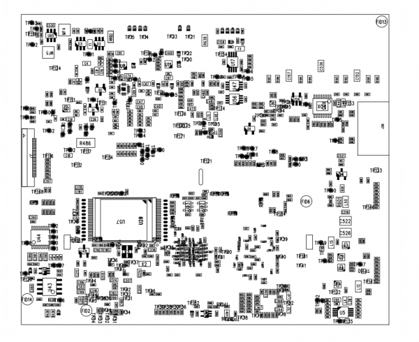
Layout[edit | edit source]
Mechanical specifications[edit | edit source]
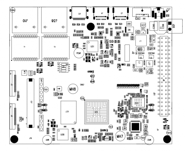
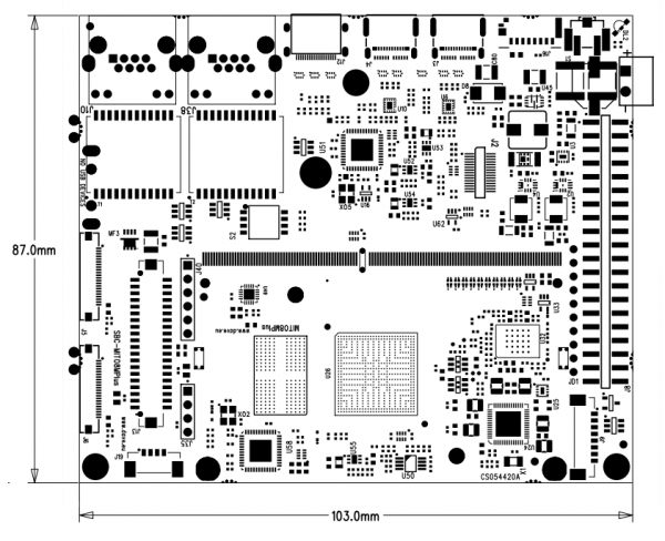
This page describes the mechanical characteristics of the ORCA SBC board.
Board layout[edit | edit source]
Dimensions[edit | edit source]
3D drawings[edit | edit source]
Mechanical data[edit | edit source]
| Dimension | Value |
|---|---|
| Width | 103 mm |
| Depth | 87 mm |
| Max component's height (top) | 13.36 mm |
| Max component's height (bottom) | 2.49 mm |
| PCB height | 1.25 mm |
