ETRA SBC/pdf
Contents
- 1 General Information
- 2 Getting started
- 3 Embedded Software Kit
- 4 Interfaces and Connectors
- 4.1 Power Supply
- 4.2 CPU connector
- 4.3 JTAG interface
- 4.4 Ethernet interface
- 4.5 Console interface
- 4.6 LCD interface
- 4.7 MIPI interface
- 4.8 micro SD interface
- 4.9 UARTs interface
- 4.10 USB ports
- 4.11 Touchscreen interface
- 4.12 RTC device
- 4.13 Watchdog peripheral
- 4.14 DWS
- 4.15 GPIOs interface
- 4.16 Auxiliary connectors interface
- 5 Electrical and Mechanical Documents
General Information[edit | edit source]
Product Highlights[edit | edit source]
The SBC ETRA platform presented here provides a compact solution for any industry and can be easily interfaced with Plant Automation Control thanks to IEC-61131 SW language environment and/or other plug-ins like QT framework or multimedia GStreamer video applications.
The following table summarizes the main hardware and software features available with SBC ETRA:
Hardware[edit | edit source]
| Subsystem | Characteristics |
|---|---|
| CPU | STMicroelectronics STM32MP1 Solo/Dual core |
| USB | Host and OTG |
| Storage | onboard eMMC or NAND, uSD connector |
| Serial Ports | dual RS232/485 port |
| Ethernet | 10/100Mbps |
| Display | WIDE™ interface with 18- or 24-bit RGB |
| Video | 2 lane MIPI interface |
| Touchscreen | USB capacitive |
| Connectivity | Bluetooth and Wi-Fi |
| LED and Buttons | (optional) membrane with up to 6 LED and 2 buttons |
| PSU | 12 to 24V DC or 5V from USB |
| Mechanical Dimensions | 87x68mm - Standard DIN (4modules) |
Software[edit | edit source]
| Subsystem | Options |
|---|---|
| Operating System | Linux |
| Distribution | Yocto |
| Graphical Framework | Qt |
Block diagram[edit | edit source]
The following picture shows a simplified block diagram of the ETRA SOM Evaluation kit.
Main functional subsystems and interfaces are depicted.

The heart of the Evaluation Kit is the ETRA SOM module: please refer to the following Product Highlights page for the Evaluation Kit product highlights information.
Here below a summary for the main characteristics of the Kit.
Features Summary[edit | edit source]
| Feature | Specifications |
|---|---|
| Supported SOM | integrated on carrier board |
| Serial Ports | 2x UART RS232/RS485 1x LVTTL UART on pin strip (debug port) |
| Connectivity | 1x 10/100TX Ethernet on RJ45 connector DWM Wireless module (optional) |
| Display | WIDE™ display interface
2 lane MIPI interface |
| Storage | 1x microSD slot
1x eMMC on board device (optional) |
| USB | 1x USB 2.0 Host port 1x USB OTG port |
| Miscellaneous | Capacitive touchscreen connector GPIOs ADCS DACs user LED and Buttons (optional) |
Electrical, Mechanical and Environmental Specifications[edit | edit source]
| Electrical / Mechanicals | Specifications |
|---|---|
| Supply voltage | + [12 - 24] V or +5V from USB OTG port |
| Dimensions | 86 mm x 68 mm |
| Weight | TBD g |
| Operating Temperature | -5/+65 °C |
Part number composition[edit | edit source]
ETRA SBC SOM module part number is identified by the following digit-code table:
| Part number structure | Options | Description |
|---|---|---|
| SDCSB | Prefix | |
| Hardware configuration |
|
Other versions can be available, please contact technical support |
| Addons, display and cameras |
|
Options like other adapters can be included - not yet coded. Other versions can be available, please contact technical support |
| Mechanical features |
|
Other versions can be available, please contact technical support |
| RFU | ||
| RFU | ||
| Temperature range |
|
Other versions can be available, please contact technical support For the DAVE Embedded Systems' product Temperature Range classification, please find more information at the page Products Classification |
| PCB revision |
|
PCB release may change for manufacturing purposes (i.e. text fixture adaptation) |
| Manufacturing option |
|
typically connected to production process and quality |
| Software Configuration | * -00: standard factory u-boot pre-programmed | If customers require custom SW deployed this section should be defined and agreed. Please contact technical support |
Example[edit | edit source]
ETRA SBC code SDCSB20100D0R-00
- SDCSB - ETRA SBC
- 2 - integrates S-DCSB20000D with the following features:
- integrates ETRA SOM DSDAE49310I Information found on the ETRA SOM Part number composition page:
- E: STM32MP157AAB3 Dual core 3D GPU -40/125°C 650MHz
- 4: 16MB
- 9: 512MB DDR3L
- 3: 8GB eMMC
- 1: on board NOR, BUS expander mount
- 0: RFU
- I: Industrial grade: suitable for 40 - 85°C envirronment
- WDT/RTC/Crypto mounted
- expansion connectors mounted
- serial connectors configured as 1x RS232, 1xRS485
- integrates ETRA SOM DSDAE49310I Information found on the ETRA SOM Part number composition page:
- 0 - no addons/displays/cameras
- 1 - No enclosure
- 0 - RFU
- 0 - RFU
- D - extended Soho Grade -5/+65°C
- 0 - first version
- R - RoHS compliant
- -00 - standard factory u-boot pre-programmed
Longevity program[edit | edit source]
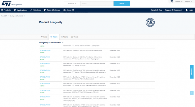
The SMT32MP1 family is included in the 10 years longevity program by ST Microelectronics
DAVE Embedded Systems is committed to provide its products at least for the same period declared by the silicon vendor. DAVE Embedded Systems manages the components' obsolescence and components through a PCN program according to JEDEC standard (where possible) which may require the customer's support.
Product life cycle termination[edit | edit source]
Once the silicon vendor provides the LBO (Last Buy Order) and LBS (Last Buy Shipment) for its products DAVE Embedded Systems provide the same documentation to its customers in order to program the product life termination.
DAVE Embedded Systems is available to continue producing the product (procuring material from after market) until the quality is granted and/or until the customer accept the extra costs related to this process.
Product continuity[edit | edit source]
DAVE Embedded Systems' goal is to grant the production continuity to its customer including the possibility to redesign its products in order to maintain the product continuity
Getting started[edit | edit source]
Unboxing[edit | edit source]
The hardware components is shown in the picture below:

The default ETRA SBC order code is SDCSB70000D1R-00 and it is composed by:
| Component | Description |
|---|---|
 |
ETRA SBC
|
| Add-ons | DWS |
| Temperature grade | Extended SoHo |
Connections[edit | edit source]
This section describes how to quick start the ETRA SBC. The picture below shows the ETRA SBC fully connected to the main peripherals:

The system is programmed to automatically boot Linux at power up, loading the bootloader, the kernel and device tree image and the root file system from the SD card memory.
To connect to the system:
- insert the SD card into the micro SD slot
- connect the 12Vcc power supply to J1 on the board
- connect the USB to TTL UART adapter to the J2 connector on the SBC and connect the USB side connector to an USB port on your computer
- if required, install the FTDI USB to serial driver
- start your favorite terminal emulator software on PC (eg: PuTTY, Minicom, ...); communication parameters are 115200,N,8,1
- (optional) connect the ethernet cable from your LAN hub/switch to the J5 RJ45 connector
- start SSH, using the following parameters:
- ip address: 192.168.0.89
- username: root
- empty password
- start SSH, using the following parameters:
Warning: please, pay attention to the debug cable header connection, see the picture here below:

First boot[edit | edit source]
Once power has been applied, U-Boot bootloader will be executed and the debug messages will be printed on the serial console. U-Boot automatically runs the autoboot macro, that loads the kernel/dtb and launches it with the options for mounting the root file system from the SD card.
At the end of the boot process, a demo application is launched and you can interact with the system using the touchscreen. The Linux shell is available on the serial console. Moreover, both telnet and ssh services are available to connect to the system through the network.
Serial console[edit | edit source]
A simple Windows serial and SSH/telnet client and terminal can be downloaded from here.
The following picture shows the serial setup for connecting to the EVK:

once selected the COM[x] serial port, click the Open button which starts the terminal. Once powered, the EVK shows the U-boot debug messages printed on the serial console.
Connecting through SSH[edit | edit source]
The following picture shows the SSH connection to the EVK:

once selected the IP address, click the Open button which starts the terminal. Once connected, the EVK shows the linux kernel prompt login for inserting the login:

Then use the root login username without password:

Boot Configurations[edit | edit source]
ETRA Evaluation Board is built upon STM32MP1 processor.
The following sections detail boot configuration options, which differ depending on the SoM.
Available options[edit | edit source]
Boot modes can be selected by S1 DIP-switch which acts directly on BOOT_MODE[2..0] configuration pins.
S1 switches are connected to ETRA BOOT_MODE[2:0] pins allowing different boot modes.

where S1 switches are mapped as the following table:
| BOOT_MODE | S1 | Note |
|---|---|---|
| BOOT_MODE0 | S1.1 | |
| BOOT_MODE1 | S1.2 | |
| BOOT_MODE2 | S1.3 | |
| - | S1.4 | USB OTG settings |
DIP settings[edit | edit source]
| BOOT_MODE[2:0] | S1[3..1] | Boot peripheral | Notes |
|---|---|---|---|
| 000 | OFF-OFF-OFF | USB | boot from USB OTG |
| 001 | OFF-OFF-ON | NOR | boot from NOR flash on Quad-SPI |
| 010 | OFF-ON-OFF | eMMC | boot from eMMC on SDMMC2 |
| 101 | ON-OFF-ON | SD | Default boot from SD card on SDMMC1 |
| 111 | ON-ON-ON | NAND | boot from NAND flash on Quad-SPI |
Reset Button[edit | edit source]
ETRA Evaluation Board has a pushbutton directly connected to the PMIC.RSTN signal which drives a PMIC hardware reset.
S2 is the hardware reset button.

Embedded Software Kit[edit | edit source]
DESK-MP1-L/Development/Hello World example
Interfaces and Connectors[edit | edit source]
Power Supply[edit | edit source]
The power supply for this EVB can be provided through J1 connector or from USB OTG connector.
Description[edit | edit source]
Power can be provided through the J1 connector. Power voltage range is +[12-24 V].
J1 is a two pins MSTBA 2.5/2-G-5.08 Phoenix connector.

Signals[edit | edit source]
The following table describes the interface signals:
| Pin# | Pin function | Pin Notes |
|---|---|---|
| 1 | VIN | +[12-24 V] |
| 2 | GND | Ground |
Power LED[edit | edit source]
DL1 is a green LED (placed near the SOM) it shows the status of the power input. This LED is ON when a valid power supply is present either from J1 or USB OTG port.
CPU connector[edit | edit source]
Description[edit | edit source]
J18 is the 204-pin SODIMM connector of the ETRA SOM.
In this SBC design, the SOM is embedded in the carrier board so the connector is not actually usable but represents the SOM J1 connector.
For a detailed description of the SOM pinout, please refer to the ETRA SOM Hardware Manual SO-DIMM connector.
JTAG interface[edit | edit source]
Description[edit | edit source]
The JTAG interface is available on the Evaluation Kit at the connector J11.
J11 is a 30 pin (2x15x2.54mm) header connector and is also used for expansion signlas.

Signals[edit | edit source]
The following table describes the interface signals on J11 connector:
| Pin# | SOM Pin# | Pin name | Pin function | Pin Notes |
|---|---|---|---|---|
| 17 | J18.62 | VDD | VDD | reference voltage |
| 19 | J18.90 | JTMS-SWDIO | JTMS-SWDIO | |
| 21 | J18.98 | JTCK-SWCLK | JTCK-SWCLK | |
| 23 | J18.92 | JTDI | JTDI | |
| 25 | J18.96 | JTDO-TRACESWOO | JTDO-TRACESWOO | |
| 27 | J18.94 | NJTRST | NJTRST |
Ethernet interface[edit | edit source]
Description[edit | edit source]
The Ethernet interface is available on the Evaluation Kit at the connector J5.
J5 is a standard RJ45 connector connected to the SOM integrated ethernet controller and PHY.
J6 and J7 connectors are pin-to-pin compatible mounting options for the same interface.

Signals[edit | edit source]
The following table describes the interface signals on J18 SOM connector:
| Pin# | SOM Pin# | Pin name | Pin function | Pin Notes |
|---|---|---|---|---|
| 3 | J18.19 | ETH_TX_P | Transmit data + | |
| 5 | J18.21 | ETH_TX_M | Transmit data - | |
| 6 | J18.23 | ETH_RX_P | Receive data + | |
| 8 | J18.25 | ETH_RX_M | Receive data - | |
| 2,11 | J18.13 | ETH1_LED | Eth link or activity led |
Device mapping[edit | edit source]
This network interface is mapped at eth0 device in Linux.
Device usage[edit | edit source]
The peripheral is used the standard kernel interface and network protocol stack.
Console interface[edit | edit source]
Description[edit | edit source]
The Console interface available on the Evaluation Kit at the connector J2.
J2 is a 4 pin (4x1x2.54mm) header connector for the two-wires USART1 port, used for debug purposes (bootloader and operating system serial console).

Signals[edit | edit source]
The following table describes the interface signals:
| Pin# | SOM Pin# | Pin name | Pin function | Pin Notes |
|---|---|---|---|---|
| 1 | J18.187 | UART TX | Transmit line | |
| 2 | J18.189 | UART RX | Receive line | |
| 3 | - | 3V3_CB | Power output | This pin can be used to power an RS232 transceiver |
| 4 | - | DGND | Ground |
Device mapping[edit | edit source]
USART1 is mapped to /dev/ttySTM0 device in Linux. The peripheral is used as the default serial console, both for the bootloader and the kernel.
Device usage[edit | edit source]
To connect to the debug serial port:
- connect the UART to USB transceiver to J2 connector
- start your favorite terminal emulator software on PC (eg: PuTTY); communication parameters are: 115200,N,8,1
LCD interface[edit | edit source]
Description[edit | edit source]
The LCD interface available on the Evaluation Kit at the connector J13.
J13 si a 40-pin, 0.5mm pitch, ZIF connector that provides the following signals:
- 18-bit RGB interface
- DE and CLK control signals
- 3.3V power for logic
- 5V power for backlight
- PWM for backlight

Signals[edit | edit source]
The following table describes the interface signals:
| Pin# | SOM Pin# | Pin name | Pin function | Pin Notes |
|---|---|---|---|---|
| 1,2,10,11,12,16,20,24,28,32,36,37,39,40 | - | GND | Ground | |
| 3 | J18.46 | LCD_PWM | PWM for backlight | |
| 4,5,6 | - | LCD_5V | 5V for LED | this rail is enabled by the CPU via GPIO |
| 7,8 | - | LCD_VDD | 3.3V for logic | this rail is enabled by the CPU via GPIO |
| 9 | J18.124 | LCD_DE | LCD_DATA_ENABLE | |
| 13 | J18.144 | LCD_B7 | LCD_B7 (MSB) | |
| 14 | J18.142 | LCD_B6 | LCD_B6 | |
| 15 | J18.140 | LCD_B5 | LCD_B5 | |
| 17 | J18.138 | LCD_B4 | LCD_B4 | |
| 18 | J18.136 | LCD_B3 | LCD_B3 | |
| 19 | J18.134 | LCD_B2 | LCD_B2 (LSB) | |
| 21 | J18.158 | LCD_G7 | LCD_G7 (MSB) | the use of this pin prevents the use of eMMC with 8bit bus |
| 22 | J18.156 | LCD_G6 | LCD_G6 | |
| 23 | J18.154 | LCD_G5 | LCD_G5 | |
| 25 | J18.152 | LCD_G4 | LCD_G4 | |
| 26 | J18.150 | LCD_G3 | LCD_G3 | |
| 27 | J18.148 | LCD_G2 | LCD_G2 (LSB) | |
| 29 | J18.172 | LCD_R7 | LCD_R7 (MSB) | |
| 30 | J18.170 | LCD_R6 | LCD_R6 | |
| 31 | J18.168 | LCD_R5 | LCD_R5 | |
| 33 | J18.166 | LCD_R4 | LCD_R4 | |
| 34 | J18.162 | LCD_R3 | LCD_R3 | |
| 35 | J18.160 | LCD_R2 | LCD_R2 (LSB) | |
| 38 | J18.132 | LCD_CLK | LCD_CLOCK |
Device mapping[edit | edit source]
LCD is mapped to /dev/fb0 device in linux.
Device usage[edit | edit source]
The connector is pinout compatible with the Ampire AM-800480BTMQW-TBMH-A display.
WARNING: the use of the LCD peripheral prevents the use of the eMMC on board of the ETRA SOM as 8bit bus, only 4bit bus is available.
The periperal can be accessed by various linux packages as fbi (for simple image display), or more complex libraries as QT or gstreamer.
Alternate connector[edit | edit source]
The ETRA SBC provides a secondary LCD connector (not mounted by default) for the use of 24bit LCD interface.
Description[edit | edit source]
The 24-bit LCD interface can be available for the Evaluation Kit at the connector J14. For the use of this interface please send an e-mail to helpdesk@dave.eu

J14 si a 40-pin, 0.5mm pitch, ZIF connector that provides the following signals:
- 24-bit RGB interface
- DE, CLK, HSYNC and VSYNC control signals
- 3.3V power for logic
- 5V power for backlight
- PWM for backlight
- two GPIO signals for panel configuration
Signals[edit | edit source]
The following table describes the interface signals:
| Pin# | SOM Pin# | Pin name | Pin function | Pin Notes |
|---|---|---|---|---|
| 9,18,27,36,40 | - | GND | Ground | |
| 1,2 | - | LCD_5V | 5V for LED | this rail is enabled by the CPU via GPIO |
| 3 | J18.46 | LCD_PWM | PWM for backlight | |
| 4 | J18.58 | LCD_5V_EN | LCD_5V power enable | can be used as GPIO if the 5V power switch is bypassed |
| 5.6 | - | LCD_VDD | 3.3V for logic | this rail is enabled by the CPU via GPIO |
| 7 | - | LCD_DISP | pull-down (default) | can be statically configured with pull-up or pull-down |
| 8 | J18.124 | LCD_DE | LCD_DATA_ENABLE | |
| 10 | J18.144 | LCD_B7 | LCD_B7 (MSB) | |
| 11 | J18.142 | LCD_B6 | LCD_B6 | |
| 12 | J18.140 | LCD_B5 | LCD_B5 | |
| 13 | J18.138 | LCD_B4 | LCD_B4 | |
| 14 | J18.136 | LCD_B3 | LCD_B3 | |
| 15 | J18.134 | LCD_B2 | LCD_B2 | |
| 16 | J18.176 | LCD_B1 | LCD_B1 | |
| 17 | J18.174 | LCD_B0 | LCD_B0 (LSB) | the use of this pin prevents the use of eMMC with 8bit bus |
| 19 | J18.158 | LCD_G7 | LCD_G7 (MSB) | the use of this pin prevents the use of eMMC with 8bit bus |
| 20 | J18.156 | LCD_G6 | LCD_G6 | |
| 21 | J18.154 | LCD_G5 | LCD_G5 | |
| 22 | J18.152 | LCD_G4 | LCD_G4 | |
| 23 | J18.150 | LCD_G3 | LCD_G3 | |
| 24 | J18.148 | LCD_G2 | LCD_G2 | |
| 25 | J18.180 | LCD_G1 | LCD_G1 | the use of this pin prevents the use of uSD with 4bit bus |
| 26 | J18.178 | LCD_G0 | LCD_G0 (LSB) | |
| 28 | J18.172 | LCD_R7 | LCD_R7 (MSB) | |
| 29 | J18.170 | LCD_R6 | LCD_R6 | |
| 30 | J18.168 | LCD_R5 | LCD_R5 | |
| 31 | J18.166 | LCD_R4 | LCD_R4 | |
| 32 | J18.162 | LCD_R3 | LCD_R3 | |
| 33 | J18.160 | LCD_R2 | LCD_R2 | |
| 34 | J18.184 | LCD_R1 | LCD_R1 | the use of this pin prevents the use of eMMC with 8bit bus |
| 35 | J18.182 | LCD_R0 | LCD_R0 (LSB) | |
| 37 | J18.130 | LCD_HSYNC | LCD_HORIZONTAL_SYNC | the use of this pin prevents the use of eMMC with 8bit bus |
| 38 | J18.132 | LCD_CLK | LCD_CLOCK | |
| 39 | J18.128 | LCD_VSYNC | LCD_VERTICAL_SYNC |
Device usage[edit | edit source]
WARNING: the use of the 24bit LCD peripheral prevents the use of the eMMC on board of the ETRA SOM as 8bit bus, only 4bit bus is available. It also prevents the use of uSD device as 4bit bus, only 1bit bus is available.
MIPI interface[edit | edit source]
Description[edit | edit source]
The MIPI Display serial Interface interface available on the Evaluation Kit at the connector J19
J19 is a 10 pin ZIF connector (0.5mm pitch, bottom contacts) for the DSI interface.

Signals[edit | edit source]
The following table describes the interface signals:
| Pin# | SOM Pin# | Pin name | Pin function | Pin Notes |
|---|---|---|---|---|
| 1 | - | DGND | Ground | |
| 2 | J18.121 | DSI_D1P | data lane1 + | |
| 3 | J18.119 | DSI_D1N | data lane1 - | |
| 4 | - | DGND | Ground | |
| 5 | J18.117 | DSI_D0P | data lane0 + | |
| 6 | J18.115 | DSI_D0N | data lane0 - | |
| 7 | - | DGND | Ground | |
| 8 | J18.113 | DSI_CKP | clock + | |
| 9 | J18.111 | DSI_CKN | clock - | |
| 10 | - | DGND | Ground |
Device mapping[edit | edit source]
The MIPI CSI peripheral is mapped to the corresponding /dev/video<X> device in Linux. The device mapping depends on the device tree configuration.
micro SD interface[edit | edit source]
Description[edit | edit source]
The micro SD interface available on the Evaluation Kit at the connector J4.
J4 is a Micro-SD card header. This interface is connected to the SDMMC1 controller of the STM32MP1 CPU.

Signals[edit | edit source]
The following table describes the interface signals:
| Pin# | SOM Pin# | Pin name | Pin function | Pin Notes |
|---|---|---|---|---|
| 1 | J18.79 | PE6 | Data 1 | |
| 2 | J18.81 | PC11 | Data 3 | |
| 3 | J18.83 | PD2 | CMD | |
| 4 | - | 3V3_SD | +3.3 V | |
| 5 | J18.85 | PC12 | Clock | |
| 6, 10 | - | DGND | Ground | |
| 7 | J18.75 | PC8 | Data 0 | |
| 8 | J18.77 | PC9 | Data 1 | |
| 11, 12, 13, 14 | - | PCB_GND_RNG | Shield | |
| 9 | J18.177 | PE9 | Card detect |
Device mapping[edit | edit source]
The microSD card is mapped to /dev/mmcblk1. The available partitions are available as /dev/mmcblk1p8, /dev/mmcblk1p9, /dev/mmcblk1p10, etc.
Device usage[edit | edit source]
The device can be mounted/accessed as a standard block device in Linux.
UARTs interface[edit | edit source]
Description[edit | edit source]
The UART interfaces are available on the Evaluation Kit at the connectors J9 and J10.
J9 and J10 are 3 pin terminal blocks 5.0mm pitch respectively for USART3 and UART8. Can be independently used as RS232 or RS485 based on Part Number composition.

Signals[edit | edit source]
The following table describes the interface signals:
J9[edit | edit source]
| Pin# | SOM Pin# | RS232 | RS485 | Pin Notes |
|---|---|---|---|---|
| 1 | J18.89 | USART3_TX | RS485_A | |
| 2 | J18.91 | USART3_RX | RS485_B | |
| 3 | - | Ground | Ground |
J10[edit | edit source]
| Pin# | SOM Pin# | RS232 | RS485 | Pin Notes |
|---|---|---|---|---|
| 1 | J18.191 | UART8_TX | RS485_A | |
| 2 | J18.193 | UART8_RX | RS485_B | |
| 3 | - | Ground | Ground |
Device mapping[edit | edit source]
USART3 is mapped to /dev/ttySTM1 device in Linux.
UART8 is mapped to /dev/ttySTM2 device in Linux.
Device usage[edit | edit source]
Fix the signal cables to the terminal with a small flat screwdriver.
USB ports[edit | edit source]
Description[edit | edit source]
ETRA SBC provides two USB ports, one HOST and one OTG:
- J17 is a standard USB HOST 2.0 Type A connector

- J16 is a micro-AB type receptacle for a USB OTG connection: this interface can operate in Host mode and Device (peripheral) mode

Signals[edit | edit source]
The following table describes the interface signals:
USB HOST[edit | edit source]
| Pin# | SOM Pin# | Pin name | Pin function | Pin Notes |
|---|---|---|---|---|
| 1 | J18.188 | USB_HOST_VBUS | VBUS | |
| 2 | J18.202 | USB_DM1 | USB Host Data - | |
| 3 | J18.200 | USB_DP1 | USB Host Data + | |
| 4 | - | DGND | Ground | |
| 5, 6, 7, 8 | - | PCB_GND_RNG | Shield |
USB OTG[edit | edit source]
| Pin# | SOM Pin# | Pin name | Pin function | Pin Notes |
|---|---|---|---|---|
| 1 | J18.185 | VBUS_OTG_IN | VBUS | Can be used to power the board |
| 2 | J18.196 | USB_DM2 | USB OTG Data - | |
| 3 | J18.198 | USB_DP2 | USB OTG Data + | |
| 4 | J18.72 | PA8 | USB OTG ID | |
| 5 | - | GND | Ground | |
| 6, 7, 8 | - | PCB_GND_RNG | Shield |
Device mapping[edit | edit source]
The USB Host port can be used under Linux for connecting USB peripheral devices: the related peripheral driver has to be integrated into the Linux kernel.
The USB OTG feature can be easily tested using the Mass Storage Gadget driver.
Touchscreen interface[edit | edit source]
Description[edit | edit source]
The Touchscreen interface is available on USB or I2C interface connectors.
ETRA Evaluation Kit uses, by default, the USB interface for connecting the touchscreen controller. Anyway, the I2C interface is available too and - optionally - can be activated in the device tree for enabling the I2C touch controller driver.
USB touchscreen[edit | edit source]
The USB OTG port - available on J16 connector - is configured as USB Host controller for driving the touchscreen. For this purpose, it is required to enable the USB OTG ID signals a low. This can be possible using the S1.4 DIP switch which forces the ID signal as low:


I2C touchscreen[edit | edit source]
The I2C touchscreen interface is available on the Evaluation Kit at the connector J20. J20 is a 6-pin Molex PicoBlade connector for the I2C and control signals needed by most of the capacitive TSC.
This interface can be configured to work with 3.3V (default) or 5V power and signal levels.

Signals[edit | edit source]
The following table describes the interface signals:
| Pin# | SOM Pin# | Pin name | Pin function | Pin Notes |
|---|---|---|---|---|
| 1 | - | DGND | Ground | |
| 2 | J18.48 | TOUCH_SDA | I2C_SDA | |
| 3 | J18.38 | TOUCH_SCL | I2C_SCL | |
| 4 | J18.101 | TOUCH_VDD | TSC power | powered through a control switch |
| 5 | J18.201 | TOUCH_INT | TSC interrupt | input |
| 6 | J18.199 | TOUCH_RES | TSC reset | output |
Device mapping[edit | edit source]
The device is typically mapped to /dev/touchscreen0 device in Linux.
The touch controller is attached to the generic Linux input event interface (evdev).
Device usage[edit | edit source]
The simplest tools for touch screen management are the tslib library and ts_tools utilities. To calibrate the touch screen, the ts_calibrate command line tool is available. After calibration, the touch screen can be tested using the graphical ts_test utility or the ts_print command line tool.
RTC device[edit | edit source]
Description[edit | edit source]
There are two RTC devices on the Evaluation Kit, one is provided by the STM32MP1 SoC, the other is a Maxim DS3232M I2C device.
Both RTC can retain time and custom data over blackouts using a backup power source as:
- the lithium rechargeable battery (BT1) optionally mounted on the carrier board
- an external battery connected to J3 (alternate mounting option to the battery)

Signals[edit | edit source]
The following table describes the interface signals for J3:
| Pin# | SOM Pin# | Pin name | Pin function | Pin Notes |
|---|---|---|---|---|
| 1 | J18.14 | VBAT | can be configured for battery connection | |
| 2 | - | DGND | Ground |
Device mapping[edit | edit source]
RTC is mapped to /dev/rtc0 device in Linux.
Device usage[edit | edit source]
The peripheral can be accessed through the date and hwclock linux commands.
Watchdog peripheral[edit | edit source]
Description[edit | edit source]
The Watchdog peripheral available on the Evaluation Kit is provided by the Maxim MAX6373.
The MAX6373 device has 3 configuration pins that allow to select the following:
- the startup delay from 3ms to 60s or first edge of the WDI signal
- the watchdog time (maximum time between WDI toggles) from 3ms to 10s or disable.
As default the device is configured for start the operations on first edge of the WDI signal with a timeout of 10s. For custom configurations please send an e-mail to helpdesk@dave.eu
Signals[edit | edit source]
The following table describes the interface signals:
| Pin# | SOM Pin# | Pin name | Pin function | Pin Notes |
|---|---|---|---|---|
| U6.1 | J18.28 | WDI | Watchdog input | |
| U6.7 | J18.24 | WDO | Watchdog output | system reset pin |
Device usage[edit | edit source]
To use the watchdog device toggle the WDI pin at least once every 5 seconds.
DWS[edit | edit source]
DWS is a Dave Wireless Module, more details at the DWS page.
Description[edit | edit source]
The DWS interface is available on the Evaluation Kit at the connector J8.
J8 is a 30-pins 0.50mm Pitch SlimStack™ Receptacle. This connector is dedicated to the DWS (optional) add-on module.
The module is built around a Telit WE866C6-P Dual Band (2.4GHz and 5GHz) 802.11 ac WiFi and Bluetooth 5 module.
The module implements the necessary PHY/MAC layers to support WLAN applications in conjunction with a host processor over a SDIO interface. The module also provides a Bluetooth platform through the HCI transport layer. Both WLAN and Bluetooth share the same antenna port.


Signals[edit | edit source]
The following table describes the interface signals:
| Pin# | SOM Pin# | Pin name | Pin function | Pin Notes |
|---|---|---|---|---|
| 1, 2 | - | 5V_CB | 5V power | |
| 3, 4 | - | 3V3_CB | 3.3V power | |
| 5, 6, 9, 10, 19 | - | DGND | Ground | |
| 7 | J18.45 | WIFI_CMD | ||
| 8 | J18.47 | WIFI_CLK | ||
| 11 | J18.37 | WIFI_DATA0 | ||
| 13 | J18.39 | WIFI_DATA1 | ||
| 15 | J18.41 | WIFI_DATA2 | ||
| 17 | J18.43 | WIFI_DATA3 | ||
| 21 | J18.80 | BT_UART_RX | Used only for BT peripheral | |
| 23 | J18.76 | BT_UART_CTS | Used only for BT peripheral | |
| 24 | J18.105 | BT_F5 | ||
| 25 | J18.74 | BT_UART_TX | Used only for BT peripheral | |
| 26 | J18.72 | BT_F2 | ||
| 27 | J18.78 | BT_UART_RTS | Used only for BT peripheral | |
| 28 | J18.70 | IRQ | ||
| 29 | J18.51 | BT_EN | ||
| 30 | J18.53 | EN | ||
| 12, 14, 16, 18, 20, 22 | - | N.C. | Not connected |
Device mapping[edit | edit source]
The WiFi peripheral is mapped to the corresponding wlan0 device in Linux. The network peripheral is visible under the ifconfig network configuration utility.
The BT peripheral is mapped to /dev/ttySTM3 device in Linux.
The control signals are managed by rfkill in Linux.
Device usage[edit | edit source]
The WiFi peripheral uses the standard kernel interface and network protocol stack.
The BT peripheral uses the standard kernel hci interface.
GPIOs interface[edit | edit source]
Description[edit | edit source]
STM32MP1 can handle external pins in many different ways and most of them can be configured as GPIOs. When a pin is set as a GPIO, it is possible to read its value, change its direction or change output value directly from the shell.

Signals[edit | edit source]
The following table describes some GPIOs signals available on J12 (2x15x2.54mm) connector:
| Pin# | SOM Pin# | Pin name | Pin function | Pin Notes |
|---|---|---|---|---|
| 3 | J18.97 | PD13 | ||
| 5 | J18.99 | PD12 | ||
| 6 | J18.34 | PB13 | ||
| 7 | J18.101 | PD11 | ||
| 8 | J18.68 | PB5 | ||
| 9 | J18.105 | PG9 | ||
| 12 | J18.48 | PA12 | ||
| 14 | J18.38 | PA11 | ||
| 18 | J18.80 | PF6 | ||
| 20 | J18.76 | PF9 | ||
| 22 | J18.74 | PF7 | ||
| 24 | J18.78 | PF8 | ||
| 26 | J18.181 | PD6 | ||
| 28 | J18.28 | PA9 |
Device mapping[edit | edit source]
GPIOs can be used directly on Linux kernel device driver or can be configured on the device tree.
Device usage[edit | edit source]
See the GPIOs page on the DESK-MP1-L Software Manual.
Auxiliary connectors interface[edit | edit source]
Description[edit | edit source]
The Auxiliary connectors on the Evaluation Kit are J11 and J12, 2x15x2.54mm stripline header.
On these connectors are available many interfaces, some of this peripherals are not available at the same time:
- FDCAN1
- FDCAN2
- I2C5
- SPI5
- UART7
- SAI2
- 11x8 keyboard matrix
- LED driver
- JTAG

Signals[edit | edit source]
The following tables describe the connectors signals:
- J11
| Pin# | SOM Pin# | Pin name | POWER | JTAG | KEYBOARD | LED |
|---|---|---|---|---|---|---|
| 1 | - | 5V_CB | 5V | |||
| 2 | - | 3V3_CB | 3.3V | |||
| 3 | J18.143 | ADP5589_R2 | ROW_2 | |||
| 4 | J18.149 | ADP5589_C0 | COLUMN_0 | LED_0 | ||
| 5 | J18.141 | ADP5589_R3 | ROW_3 | |||
| 6 | J18.151 | ADP5589_C1 | COLUMN_1 | LED_1 | ||
| 7 | J18.139 | ADP5589_R4 | ROW_4 | |||
| 8 | J18.155 | ADP5589_C2 | COLUMN_2 | LED_2 | ||
| 9 | J18.137 | ADP5589_R5 | ROW_5 | |||
| 10 | J18.157 | ADP5589_C3 | COLUMN_3 | LED_3 | ||
| 11 | J18.135 | ADP5589_R6 | ROW_6 | |||
| 12 | J18.159 | ADP5589_C4 | COLUMN_4 | LED_4 | ||
| 13 | J18.133 | ADP5589_R7 | ROW_7 | |||
| 14 | J18.161 | ADP5589_C5 | COLUMN_5 | LED_5 | ||
| 15,20,29 | - | DGND | Ground | |||
| 16 | J18.147 | ADP5589_R0 | ROW_0 | |||
| 17 | - | VDD | 3.3V | ref. voltage | ||
| 18 | J18.145 | ADP5589_R1 | ROW_1 | |||
| 19 | J18.90 | JTMS-SWDIO | JTMS-SWDIO | |||
| 21 | J18.98 | JTCK-SWCLK | JTCK-SWCLK | |||
| 22 | J18.163 | ADP5589_C6 | COLUMN_6 | |||
| 23 | J18.92 | JTDI | JTDI | |||
| 24 | J18.165 | ADP5589_C7 | COLUMN_7 | |||
| 25 | J18.96 | JTDO-TRACESWOO | JTDO-TRACESWOO | |||
| 26 | J18.167 | ADP5589_C8 | COLUMN_8 | |||
| 27 | J18.94 | NJTRST | NJTRST | |||
| 28 | J18.169 | ADP5589_C9 | COLUMN_9 | |||
| 30 | J18.171 | ADP5589_C10 | COLUMN_10 |
- J12
| Pin# | SOM Pin# | Pin name | POWER | System control | CAN | I2C | SPI | UART | SAI |
|---|---|---|---|---|---|---|---|---|---|
| 1 | - | 5V_CB | 5V | ||||||
| 2,4 | - | PMIC_3V3 | 3.3V | ||||||
| 3 | J18. | PD13 | SAI2_SCK_A | ||||||
| 5 | J18. | PD12 | SAI2_FS_A | ||||||
| 6 | J18. | PB13 | FDCAN2_TX | ||||||
| 7 | J18. | PD11 | SAI2_SD_A | ||||||
| 8 | J18. | PB5 | FDCAN2_RX | ||||||
| 9 | J18. | PG9 | SAI2_FS_B | ||||||
| 10, 11, 16, 19, 29, 30 | - | DGND | Ground | ||||||
| 12 | J18. | PA12 | FDCAN1_TX | I2C5_SDA | |||||
| 13 | - | 3V3_CB | 3.3V | ||||||
| 14 | J18. | PA11 | FDCAN1_RX | I2C5_SCL | |||||
| 15 | - | N.C. | |||||||
| 17 | - | N.C. | |||||||
| 18 | J18. | PF6 | SPI5_NSS | UART7_RX | |||||
| 20 | J18. | PF9 | SPI5_MOSI | UART7_CTS | |||||
| 21 | J18. | NRST | system reset | ||||||
| 22 | J18. | PF7 | SPI5_SCK | UART7_TX | |||||
| 23 | J18. | PONKEYn | power key | ||||||
| 24 | J18. | PF8 | SPI5_MISO | UART7_RTS/
UART7_DE |
|||||
| 25 | J18. | EEPROM_WP | write protect for carrier eeprom | ||||||
| 26 | J18. | PD6 | |||||||
| 27 | J18. | MEM_WP# | write protect for NAND | ||||||
| 28 | J18. | PA9 |
Device usage[edit | edit source]
CAN[edit | edit source]
The CAN interfaces need a tranceiver to be connected to the CAN bus.
NOTE: the FDCAN1 pins are shared with touchscreen I2C interface and are not available when using I2C5.
See the CAN page for more informations.
I2C5[edit | edit source]
Configured by deafult for touchscreen I2C interface.
See the I2C page for more informations.
SPI5[edit | edit source]
NOTE: these pins are shared with UART7, cannot be used at the same time.
See the SPI page for more informations.
UART7[edit | edit source]
NOTE: these pins are shared with SPI5, cannot be used at the same time.
See the UART page for more informations.
SAI2[edit | edit source]
See the Audio page for more informations.
LED driver[edit | edit source]
Open collector outputs through a 120ohm resistor. Can be drive indicators LEDs
By default all the pins are available.
keyboard matrix[edit | edit source]
NOTE: COLUMN[0:5] are not available by default as the pins are routed to the LED open collector outputs. Please send an e-mail to helpdesk@dave.eu for custom configurations.
See the IO_expander page for more informations.
Interface membrane[edit | edit source]
This mambrane can be provided for user interface when the system is mounted on the 4 modules DIN BAR profile, it can offer up to 2 keys and 6 LEDs.
Please send an e-mail to helpdesk@dave.eu for more informations.
JTAG[edit | edit source]
See the JTAG page for more informations.
System control[edit | edit source]
See the reset scheme for more informations.
The system control signals are the following:
- system reset
- tie to ground for reset the system
- power key
- tie to ground for power up and down the system
- write protect for carrier eeprom
- tie to ground for write inside the carrier eeprom
- the first 32 bytes of the eeprom are used to store the CB ConfigID, the corruption of these bytes prevents the system from boot.
- write protect for NAND
- this pin allow to prevent unwanted writes, tie to ground when the NAND are not to be written.
Electrical and Mechanical Documents[edit | edit source]
Please find here below the links for the ETRA Evaluation Kit schematics and the related documents (BOM and layout).
 Please note that SBC ETRA has been built around the ETRA SOM: on page 12 there is the SO-DIMM connector which separates the inside SOM core vs the external SBC. The SOM schematics are reserved and not published as documentation. |
Schematics[edit | edit source]
Layout[edit | edit source]
Mechanical specifications[edit | edit source]
This page describes the mechanical characteristics of the ETRA SBC board.
Board layout[edit | edit source]


Dimensions[edit | edit source]

3D drawings[edit | edit source]
Mechanical data[edit | edit source]
| Dimension | Value |
|---|---|
| Width | 87 mm |
| Depth | 68 mm |
| Max component's height (top) | - mm |
| Max component's height (bottom) | |
| PCB height | - mm |