DWS ADD-ON/DWS Hardware/pdf
General Information[edit | edit source]
DWS TOP View[edit | edit source]

DWS BOTTOM View[edit | edit source]

Introduction[edit | edit source]
The module is built around a Telit WE866C6-P Dual Band (2.4GHz and 5GHz) 802.11 ac WiFi and Bluetooth 5 module. The module implements the necessary PHY/MAC layers to support WLAN applications in conjunction with a host processor over a SDIO interface. The module provides a Bluetooth platform through the HCI transport layer. Both WLAN and Bluetooth share the same antenna port.
Features[edit | edit source]
- Based on Telit WE866C6-P
- Wi-Fi - 802.11 a/b/g/n/ac (dual band 2.4GHz and 5GHz)
- Bluetooth BLE 5 with low energy (LE) support
- Reduced footprint: 25 mm x 38 mm
- Low height profile
- U.FL connector for external antenna
- Integrated LTE-Wi-Fi/BLE coexistence filter
- Additional PCM interface for BT Audio (optional)
- Industrial operating temperature range: -40 / +85 °C
Interface timings[edit | edit source]
Please refer to the WE866C6-P Datasheet for SDIO 3.0 [WiFi] and UART [Bluetooth] interface timings.
Hardware versioning and tracking[edit | edit source]
DWS SOM implements well established versioning and tracking mechanisms:
- PCB version is copper printed on PCB itself, as shown in Fig. 1
- serial number: it is printed on a white label, as shown in Fig. 2: see also Product serial number page for more details

Part number composition[edit | edit source]
DWS ADD-ON part number is identified by the following digit-code table:
| Part number structure | Options | Description |
|---|---|---|
| Family | DWS | Family prefix code |
| Chipset |
|
|
| RFU |
|
Reserved for future use |
| RFU |
|
Reserved for future use |
| Form factor |
|
|
| Temperature range |
|
For the DAVE Embedded Systems' product Temperature Range classification, please find more information at the page Products Classification |
| PCB revision |
|
PCB release may change for manufacturing purposes (i.e. text fixture adaptation) |
| Manufacturing option |
|
typically connected to production process and quality |
| Software Configuration |
|
If customers require custom SW deployed this section should be defined and agreed |
Example[edit | edit source]
DWS ADD-ON code DWS0000I0R-00
- DWS - DWS ADD-ON
- 0 - WE866C6 chipset
- 000 - standard version
- I - Industrial temperature range (i.e. -40 to 85°C)
- 0 - First PCB revision
- R - RoHS manufacturing process
- -00 default
Pinout Table[edit | edit source]
Connectors and Pinout Table[edit | edit source]
Connectors description[edit | edit source]
In the following table are described all available connectors integrated on DWS_ADD-ON:
| Connector name | Connector Type | Notes | Carrier board counterpart |
|---|---|---|---|
| J1 | Dual in line low profile high density connector 30pins | Molex 501920-3001 | Molex 52991-030, others are available with different stand-off |
| Antenna's connector | UFL type | N.A. | UFL cable side (many versions available in the market already inserted on cables/antenna patches) |
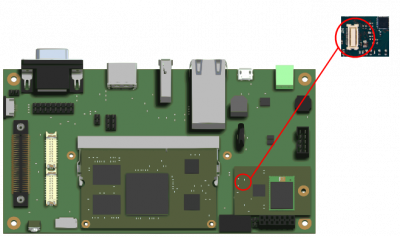
The dedicated carrier board must mount the mating connector and connect the desired peripheral interfaces according to DWS pinout specifications. See the images below for reference:
Pinout table naming conventions[edit | edit source]
This chapter contains the pinout description of the DWS module, grouped in two tables (odd and even pins) that report the pin mapping of the TBD: connector type DWS connector.
Each row in the pinout tables contains the following information:
| Pin | Reference to the connector pin |
| Pin Name | Pin (signal) name on the DWS connectors |
| Internal connections |
Connections to the DWS components
|
| Ball/pin # | Component ball/pin number connected to signal |
| Voltage | I/O voltage levels |
| Type | Pin type:
|
| Notes | Remarks on special pin characteristics |
| Pin MUX alternative functions | Muxes:
The number of functions depends on platform |
Pinout Table ODD pins declaration[edit | edit source]
| Pin | Pin Name | Internal Connections | Ball/pin # | Voltage domain | Type | Notes | Pin MUX alternative functions |
| J1.1 | BT_EN | Bluetooth Enable | 3.3V | I | |||
| J1.3 | BT_CTS | Bluetooth HCI UART CTS | 3.3V | I | |||
| J1.5 | BT_RX | Bluetooth HCI UART RX | 3.3V | I | |||
| J1.7 | BT_RTS | Bluetooth HCI UART RTS | 3.3V | O | |||
| J1.9 | BT_TX | Bluetooth HCI UART TX | 3.3V | O | |||
| J1.11 | DGND | Ground | - | G | |||
| J1.13 | SDIO_DAT3 | SDIO Data Bit 3 | 3.3V | I/O | |||
| J1.15 | SDIO_DAT2 | SDIO Data Bit 2 | 3.3V | I/O | |||
| J1.17 | SDIO_DAT1 | SDIO Data Bit 1 | 3.3V | I/O | |||
| J1.19 | SDIO_DAT0 | SDIO Data Bit 0 | 3.3V | I/O | |||
| J1.21 | DGND | Ground | - | G | |||
| J1.23 | SDIO_CMD | SDIO Command Line | 3.3V | I/O | |||
| J1.25 | DGND | Ground | - | G | |||
| J1.27 | 3.3V | +3.3V Input Voltage | 3.3V | S | |||
| J1.29 | 5V | +5V Input Voltage | 5V | S | Not used on default mounting option |
Pinout Table EVEN pins declaration[edit | edit source]
| Pin | Pin Name | Internal Connections | Ball/pin # | Voltage domain | Type | Note | Pin MUX alternative functions |
| J1.2 | WIFI_EN | WLAN Enable | 3.3V | I | |||
| J1.4 | WIFI_IRQ | WOW (Wake On Wireless) | 3.3V | O | Open drain output with internal pull-up
Do Not Connect on the carrier board (this feature is not supported yet) |
||
| J1.6 | BT_F2 | Reserved for future use | - | Do Not Connect on the carrier board | |||
| J1.8 | WIFI_CLK_REQ(A) | Reserved for future use | - | Do Not Connect on the carrier board | |||
| J1.10 | NC | Reserved for future use | - | Do Not Connect on the carrier board | |||
| J1.12 | NC | Reserved for future use | - | Do Not Connect on the carrier board | |||
| J1.14 | AUDIO_I2S_SDO | Reserved for future use | - | Do Not Connect on the carrier board | |||
| J1.16 | AUDIO_I2S_SCK | Reserved for future use | - | Do Not Connect on the carrier board | |||
| J1.18 | AUDIO_I2S_WS | Reserved for future use | - | Do Not Connect on the carrier board | |||
| J1.20 | AUDIO_I2S_SDI | Reserved for future use | - | Do Not Connect on the carrier board | |||
| J1.22 | DGND | Ground | - | G | |||
| J1.24 | SDIO_CLK | SDIO Clock | 3.3V | I | |||
| J1.26 | DGND | Ground | - | G | |||
| J1.28 | 3.3V | +3.3V Input Voltage | 3.3V | S | |||
| J1.30 | 5V | +5V Input Voltage | 5V | S | Not connected/used on default mounting option |
Integration guide[edit | edit source]
Integration guide[edit | edit source]
This section provides useful information and resources that let the system designer integrate the DWS module in the application very quickly.
Typical scenario[edit | edit source]
The following picture shows the conceptual block diagram of the application where the host is an Embedded System.

Electrical guidelines[edit | edit source]
- SDIO lines
- 50ohm single ended impedance
- keep lines as short as possible
- place series resistor on the carrier for impedance matching (tipical 22ohm)
- 5V and 3.3V rails can power up in any order
- by default 5V rail is not used by the add-on
- keep WIFI_EN asserted during power-up sequence
Customizations[edit | edit source]
Many customization are potentially available for this module:
- I/O with 1.8V levels
- applies to all the interfaces (SDIO, UART, EN)
- the module can be powered by the 5V rail only
- I2S interface can be made available for BT operations
Ask more information to technical support about this topic.
Calibration process[edit | edit source]
The radio interface of the DWS module is configured by several parameters. These parameters are set in Linux user space.
Regulatory domain[edit | edit source]
For proper operation in the country where the system is deployed, the regulatory domain has to be configured. See this section for more details
MAC address[edit | edit source]
The MAC address is fused inside the module and assured to be unique
Antenna selection[edit | edit source]
The WiFi module featured inside this add-on provides some precertifications that allow the final customer to decrease the amount of test to perform to obtain the needed certification.
To be able to use these precertifications a proper antenna has to be selected. Refer to the manufacturer Hardware Design Guide, linked in the References section of this page, or contact technical support for more informations.
Tested Antennas[edit | edit source]
Following a list of tested and approved antennas:
- Atel T-AT9552 with UFL to SMA adapter:
- J2 Antennas 2JF0102P patch antenna


The antenna 1. has been used by the manufacturer for the precertification tests
The antenna 2. has been used by DAVE for the qualification tests
References[edit | edit source]
- WE866C6-P Wi-Fi module manufacturer's documentation page
- see the Hardware Design Guide for the antenna selection
- see the Wi-Fi and Bluetooth Network Interface Card NIC User Guide for software implementations
Electrical, Thermal and Mechanical Features[edit | edit source]
Operational characteristics[edit | edit source]
Maximum ratings[edit | edit source]
| Parameter | Min | Typ | Max | Unit |
|---|---|---|---|---|
| 3.3V power supply voltage | -0.3 | 3.3 | 3.65 | V |
| 5V power supply voltage | -0.3 | 5 | 6.5 | V |
Recommended ratings[edit | edit source]
| Parameter | Min | Typ | Max | Unit |
|---|---|---|---|---|
| 3.3V power supply voltage | 3.135 | 3.3 | 3.46 | V |
| 5V power supply voltage | 3.525 | 5 | 6 | V |
By default 5V power supply voltage is not used inside the add-on, see integration guide for more informations.
Mechanical specifications[edit | edit source]
This chapter describes the mechanical characteristics of the DWS module.
Board Layout[edit | edit source]
The following figure shows the physical dimensions of the DWS module:

Connectors[edit | edit source]
The following figure shows the DWS connector layout:


CAD drawings[edit | edit source]
3D drawings[edit | edit source]