General InformationEdit
DWS TOP ViewEdit

DWS BOTTOM ViewEdit

IntroductionEdit
The module is built around a Telit WE866C6-P Dual Band (2.4GHz and 5GHz) 802.11 ac WiFi and Bluetooth 5 module. The module implements the necessary PHY/MAC layers to support WLAN applications in conjunction with a host processor over a SDIO interface. The module provides a Bluetooth platform through the HCI transport layer. Both WLAN and Bluetooth share the same antenna port.
FeaturesEdit
- Based on Telit WE866C6-P
- Wi-Fi - 802.11 a/b/g/n/ac (dual band 2.4GHz and 5GHz)
- Bluetooth BLE 5 with low energy (LE) support
- Reduced footprint: 25 mm x 38 mm
- Low height profile
- U.FL connector for external antenna
- Integrated LTE-Wi-Fi/BLE coexistence filter
- Additional PCM interface for BT Audio (optional)
- Industrial operating temperature range: -40 / +85 °C
Interface timingsEdit
Please refer to the WE866C6-P Datasheet for SDIO 3.0 [WiFi] and UART [Bluetooth] interface timings.
Hardware versioning and trackingEdit
DWS SOM implements well established versioning and tracking mechanisms:
- PCB version is copper printed on PCB itself, as shown in Fig. 1
- serial number: it is printed on a white label, as shown in Fig. 2: see also Product serial number page for more details

Part number compositionEdit
DWS ADD-ON part number is identified by the following digit-code table:
| Part number structure | Options | Description |
|---|---|---|
| Family | DWS | Family prefix code |
| Chipset |
|
|
| RFU |
|
Reserved for future use |
| RFU |
|
Reserved for future use |
| Form factor |
|
|
| Temperature range |
|
For the DAVE Embedded Systems' product Temperature Range classification, please find more information at the page Products Classification |
| PCB revision |
|
PCB release may change for manufacturing purposes (i.e. text fixture adaptation) |
| Manufacturing option |
|
typically connected to production process and quality |
| Software Configuration |
|
If customers require custom SW deployed this section should be defined and agreed |
ExampleEdit
DWS ADD-ON code DWS0000I0R-00
- DWS - DWS ADD-ON
- 0 - WE866C6 chipset
- 000 - standard version
- I - Industrial temperature range (i.e. -40 to 85°C)
- 0 - First PCB revision
- R - RoHS manufacturing process
- -00 default
Pinout TableEdit
Connectors and Pinout TableEdit
Connectors descriptionEdit
In the following table are described all available connectors integrated on DWS_ADD-ON:
| Connector name | Connector Type | Notes | Carrier board counterpart |
|---|---|---|---|
| J1 | Dual in line low profile high density connector 30pins | Molex 501920-3001 | Molex 52991-030, others are available with different stand-off |
| Antenna's connector | UFL type | N.A. | UFL cable side (many versions available in the market already inserted on cables/antenna patches) |
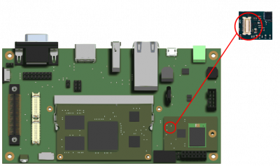
The dedicated carrier board must mount the mating connector and connect the desired peripheral interfaces according to DWS pinout specifications. See the images below for reference:
Pinout table naming conventionsEdit
This chapter contains the pinout description of the DWS module, grouped in two tables (odd and even pins) that report the pin mapping of the TBD: connector type DWS connector.
Each row in the pinout tables contains the following information:
| Pin | Reference to the connector pin |
| Pin Name | Pin (signal) name on the DWS connectors |
| Internal connections |
Connections to the DWS components
|
| Ball/pin # | Component ball/pin number connected to signal |
| Voltage | I/O voltage levels |
| Type | Pin type:
|
| Notes | Remarks on special pin characteristics |
| Pin MUX alternative functions | Muxes:
The number of functions depends on platform |
Pinout Table ODD pins declarationEdit
| Pin | Pin Name | Internal Connections | Ball/pin # | Voltage domain | Type | Notes | Pin MUX alternative functions |
| J1.1 | BT_EN | Bluetooth Enable | 3.3V | I | |||
| J1.3 | BT_CTS | Bluetooth HCI UART CTS | 3.3V | I | |||
| J1.5 | BT_RX | Bluetooth HCI UART RX | 3.3V | I | |||
| J1.7 | BT_RTS | Bluetooth HCI UART RTS | 3.3V | O | |||
| J1.9 | BT_TX | Bluetooth HCI UART TX | 3.3V | O | |||
| J1.11 | DGND | Ground | - | G | |||
| J1.13 | SDIO_DAT3 | SDIO Data Bit 3 | 3.3V | I/O | |||
| J1.15 | SDIO_DAT2 | SDIO Data Bit 2 | 3.3V | I/O | |||
| J1.17 | SDIO_DAT1 | SDIO Data Bit 1 | 3.3V | I/O | |||
| J1.19 | SDIO_DAT0 | SDIO Data Bit 0 | 3.3V | I/O | |||
| J1.21 | DGND | Ground | - | G | |||
| J1.23 | SDIO_CMD | SDIO Command Line | 3.3V | I/O | |||
| J1.25 | DGND | Ground | - | G | |||
| J1.27 | 3.3V | +3.3V Input Voltage | 3.3V | S | |||
| J1.29 | 5V | +5V Input Voltage | 5V | S | Not used on default mounting option |
Pinout Table EVEN pins declarationEdit
| Pin | Pin Name | Internal Connections | Ball/pin # | Voltage domain | Type | Note | Pin MUX alternative functions |
| J1.2 | WIFI_EN | WLAN Enable | 3.3V | I | |||
| J1.4 | WIFI_IRQ | WOW (Wake On Wireless) | 3.3V | O | Open drain output with internal pull-up
Do Not Connect on the carrier board (this feature is not supported yet) |
||
| J1.6 | BT_F2 | Reserved for future use | - | Do Not Connect on the carrier board | |||
| J1.8 | WIFI_CLK_REQ(A) | Reserved for future use | - | Do Not Connect on the carrier board | |||
| J1.10 | NC | Reserved for future use | - | Do Not Connect on the carrier board | |||
| J1.12 | NC | Reserved for future use | - | Do Not Connect on the carrier board | |||
| J1.14 | AUDIO_I2S_SDO | Reserved for future use | - | Do Not Connect on the carrier board | |||
| J1.16 | AUDIO_I2S_SCK | Reserved for future use | - | Do Not Connect on the carrier board | |||
| J1.18 | AUDIO_I2S_WS | Reserved for future use | - | Do Not Connect on the carrier board | |||
| J1.20 | AUDIO_I2S_SDI | Reserved for future use | - | Do Not Connect on the carrier board | |||
| J1.22 | DGND | Ground | - | G | |||
| J1.24 | SDIO_CLK | SDIO Clock | 3.3V | I | |||
| J1.26 | DGND | Ground | - | G | |||
| J1.28 | 3.3V | +3.3V Input Voltage | 3.3V | S | |||
| J1.30 | 5V | +5V Input Voltage | 5V | S | Not connected/used on default mounting option |
Integration guideEdit
Integration guideEdit
This section provides useful information and resources that let the system designer integrate the DWS module in the application very quickly.
Typical scenarioEdit
The following picture shows the conceptual block diagram of the application where the host is an Embedded System.

Electrical guidelinesEdit
- SDIO lines
- 50ohm single ended impedance
- keep lines as short as possible
- place series resistor on the carrier for impedance matching (tipical 22ohm)
- 5V and 3.3V rails can power up in any order
- by default 5V rail is not used by the add-on
- keep WIFI_EN asserted during power-up sequence
CustomizationsEdit
Many customization are potentially available for this module:
- I/O with 1.8V levels
- applies to all the interfaces (SDIO, UART, EN)
- the module can be powered by the 5V rail only
- I2S interface can be made available for BT operations
Ask more information to technical support about this topic.
Calibration processEdit
The radio interface of the DWS module is configured by several parameters. These parameters are set in Linux user space.
Regulatory domainEdit
For proper operation in the country where the system is deployed, the regulatory domain has to be configured. See this section for more details
MAC addressEdit
The MAC address is fused inside the module and assured to be unique
Antenna selectionEdit
The WiFi module featured inside this add-on provides some precertifications that allow the final customer to decrease the amount of test to perform to obtain the needed certification.
To be able to use these precertifications a proper antenna has to be selected. Refer to the manufacturer Hardware Design Guide, linked in the References section of this page, or contact technical support for more informations.
Tested AntennasEdit
Following a list of tested and approved antennas:
- Atel T-AT9552 with UFL to SMA adapter:
- J2 Antennas 2JF0102P patch antenna


The antenna 1. has been used by the manufacturer for the precertification tests
The antenna 2. has been used by DAVE for the qualification tests
ReferencesEdit
- WE866C6-P Wi-Fi module manufacturer's documentation page
- see the Hardware Design Guide for the antenna selection
- see the Wi-Fi and Bluetooth Network Interface Card NIC User Guide for software implementations
Electrical, Thermal and Mechanical FeaturesEdit
Operational characteristicsEdit
Maximum ratingsEdit
| Parameter | Min | Typ | Max | Unit |
|---|---|---|---|---|
| 3.3V power supply voltage | -0.3 | 3.3 | 3.65 | V |
| 5V power supply voltage | -0.3 | 5 | 6.5 | V |
Recommended ratingsEdit
| Parameter | Min | Typ | Max | Unit |
|---|---|---|---|---|
| 3.3V power supply voltage | 3.135 | 3.3 | 3.46 | V |
| 5V power supply voltage | 3.525 | 5 | 6 | V |
By default 5V power supply voltage is not used inside the add-on, see integration guide for more informations.
Mechanical specificationsEdit
This chapter describes the mechanical characteristics of the DWS module.
Board LayoutEdit
The following figure shows the physical dimensions of the DWS module:

ConnectorsEdit
The following figure shows the DWS connector layout:

