|
|
| (110 intermediate revisions by 4 users not shown) |
| Line 1: |
Line 1: |
| | {{InfoBoxTop}} | | {{InfoBoxTop}} |
| | {{AppliesToDacu}} | | {{AppliesToDacu}} |
| − | {{AppliesToAxel}}
| |
| − | {{AppliesToAxelLite}}
| |
| − | {{AppliesToAxelEsatta}}
| |
| − | {{Applies To Diva}}
| |
| | {{AppliesToLizard}} | | {{AppliesToLizard}} |
| | {{InfoBoxBottom}} | | {{InfoBoxBottom}} |
| | | | |
| − | ==Introduction== | + | ===Introduction=== |
| | | | |
| − | [[File:Dacu-top-view.png|600px|frameless|border]] | + | Dacu is an ARM Cortex-A8 industrial tablet platform, built around a carrier board hosting the [[:Category:Lizard|Lizard]] CPU module |
| | | | |
| − | Dacu is a '''carrier board''' that can host various '''DAVE Embedded Systems''' SOMs, like, for example, the [[:Category:Lizard|Lizard]] CPU module. | + | The following picture shows block diagram of Dacu: |
| − | {{ImportantMessage|text=Please note that DACU supports several BOM variants in order to mate with different SOMs or evaluation boards.}}
| + | [[File:dacu-bd.jpg|thumbnail|center]] |
| | | | |
| | + | ===Quick start=== |
| | + | This section describes how to quick start Dacu system. |
| | | | |
| − | Dacu's system specifications are the following:
| |
| | | | |
| − | {| class="wikitable"
| + | ==== "Full control" mode ==== |
| − | |-
| + | # connect the serial cable, provided with the board, to J3 pin-strip connector |
| − | |Supported SOMs
| + | # connect this cable to PC COM port through a NULL-modem cable (not provided) |
| − | |[[:Category:AxelUltra|Axel Ultra]]<br>[[:Category:AxelLite|Axel Lite]]<br>[[:Category:Diva|Diva]]<br>[[:Category:Lizard|Lizard]]
| + | # start your favourite terminal software on PC; communication parameters are: |
| − | |-
| + | #* baud rate: 115200 Bps |
| − | |Power
| + | #* data bits: 8 |
| − | |12-24 V
| + | #* stop bits: 1 |
| − | |-
| + | #* parity: none |
| − | |Serial Ports
| + | # connect the system to Ethernet LAN (RJ45 connector, J6) |
| − | |1x UART RS232 on DB9<br>1x UART (RS232/RS422/RS485) or CAN on DB9 (hardware mount options)<br>1x UART RS232 on pin strip (debug port)
| + | # connect a 12Vcc power supply to to the power jack (JP2) |
| − | |-
| |
| − | |Ethernet
| |
| − | |1x Fast Ethernet on RJ45 connector
| |
| − | |-
| |
| − | |Display
| |
| − | |7" 800x480 LVDS
| |
| − | |-
| |
| − | |Storage
| |
| − | |1x microSD slot
| |
| − | |-
| |
| − | |USB
| |
| − | |2x USB 2.0 ports
| |
| − | |-
| |
| − | |Audio
| |
| − | |UDA1345 codec
| |
| − | |-
| |
| − | |Buses
| |
| − | |I2C<br>SPI
| |
| − | |-
| |
| − | |Other
| |
| − | |On board touch controller<br>Optional Wi-Fi module<br>GPIOs
| |
| − | |-
| |
| − | |}
| |
| | | | |
| − | == Block Diagram ==
| + | Once power has been applied, U-Boot bootloader will be executed and the following messages will be printed on serial console: |
| | | | |
| − | The following picture shows block diagram of the Dacu carrier board (the version for the Lizard SOM):
| + | <pre class="board-terminal"> |
| | + | U-Boot 2009.11-00074-g34e0d5b-dirty (Jul 17 2012 - 11:00:55) [dacu-android-0.9.2] |
| | | | |
| − | [[File:dacu-bd.png|thumbnail|center|400px]]
| + | AM35xx-GP ES2.0, L3-165MHz |
| | + | DAVE Lizard board + LPDDR/NAND |
| | + | I2C: ready |
| | + | DRAM: 256 MB |
| | + | Flash: 32 MB |
| | + | NAND: 1024 MiB |
| | + | In: serial |
| | + | Out: serial |
| | + | Err: serial |
| | + | Die ID #7cf60001000000000160ae2d0b01e00a |
| | + | Net: davinci_emac_initialize |
| | + | Ethernet PHY: GENERIC @ 0x11 |
| | + | DaVinci EMAC |
| | + | Hit any key to stop autoboot: 0 |
| | + | => |
| | | | |
| − | == Mechanicals ==
| + | </pre> |
| | | | |
| − | The following picture shows the mechanical layout of Dacu:
| + | Once the boot process has completed, you'll get the default Android "desktop": |
| − | [[File:Dacu-top.png|thumbnail|center|400px]]
| |
| | | | |
| − | == Available options ==
| + | [[File:Android-dacu-lock-screen.jpg|thumb|none|border|450px|Android default lock screen]] |
| | | | |
| − | === RS232/RS485/RS422 or CAN ===
| + | Moreover, you'll have immediate access to the Android shell, so you can use the shell commands to interact with the system and see the output messages on the console. Using the serial console doesn't prevent you from using also the adb tool to access the system. |
| | | | |
| − | === Male or female DB9 connector === | + | ==== "Normal" mode ==== |
| | + | # connect the system to Ethernet LAN (RJ45 connector, J6) |
| | + | # connect a 12Vcc power supply to to the power jack (JP2) |
| | | | |
| − | == Connectors pinout ==
| + | Once power has been applied, the system will boot loading the software components from the internal flash. Once the boot process has completed, you'll get the default Android "desktop": |
| | | | |
| − | The following section describes the on-board connectors and their pinout.
| + | You can now access the system using adb. |
| | | | |
| − | === Power supply ===
| |
| | | | |
| − | Power is provided through the JP2 DC Power Jack. Power voltage range is [12-24 V]
| + | ==== Running the Android Debug Bridge (ADB) ==== |
| | | | |
| − | === CPU module connectors – J1, J2 ===
| + | [http://developer.android.com/tools/help/adb.html ADB] is a fundamental development tool and enables remote access to the Android device. ADB is provided with the Android SDK, so before using it you must install the SDK. |
| | | | |
| − | J1 and J2 are the 140-pin mating connectors for the hosted SOM.
| + | To establish the ADB connection, on a Linux host machine launch the following commands: |
| | | | |
| − | === UART1 - J4 === | + | <pre class="workstation-terminal"> |
| | + | $ export PATH=${PATH}:<your_sdk_dir>/platform-tools |
| | + | $ export ADBHOST=<target's ip address> |
| | + | $ adb kill-server |
| | + | $ adb start-server |
| | + | </pre> |
| | | | |
| − | J4 is a standard DB9 connector for the RS232 four-wires UART1 port. The following table reports the connector's pinout:
| + | To check the connection, please launch |
| | | | |
| − | {| class="wikitable"
| + | <pre class="workstation-terminal"> |
| − | |-
| + | $ adb devices |
| − | !Pin#
| + | </pre> |
| − | !Pin name
| |
| − | !Function
| |
| − | !Notes
| |
| − | |-
| |
| − | |1, 4, 6, 9
| |
| − | |N.A.
| |
| − | |N.A.
| |
| − | |Connected to protection diode array
| |
| − | |-
| |
| − | |2
| |
| − | |UART_EXT_RX
| |
| − | |Receive line
| |
| − | |
| |
| − | |-
| |
| − | |3
| |
| − | |UART_EXT_TX
| |
| − | |Transmit line
| |
| − | |
| |
| − | |-
| |
| − | |5
| |
| − | |DGND
| |
| − | |Ground
| |
| − | |
| |
| − | |-
| |
| − | |7
| |
| − | |UART_EXT_RTS
| |
| − | |Request To Send line
| |
| − | |
| |
| − | |-
| |
| − | |8
| |
| − | |UART_EXT_CTS
| |
| − | |Clear To Send line
| |
| − | |
| |
| − | |-
| |
| − | |}
| |
| | | | |
| − | === UART2/CAN - J5 ===
| + | If everything is working properly, you should see the following messages: |
| | | | |
| − | J5 is a standard DB9 '''male''' connector for the configurable UART/CAN port. The board provides some '''hardware''' mount options for the selection of the UART mode (RS232/RS422/RS485 with auto-direction) or the CAN mode. The board default configuration provides the CAN interface on this port, while the RS232/RS422/RS485 interface is provided as an option to customers who choose the alternative configuration.
| + | <pre class="workstation-terminal"> |
| | + | $ adb devices |
| | + | List of devices attached |
| | + | emulator-5554 device |
| | + | </pre> |
| | | | |
| − | Please note that this port can be used to connect a [http://www.rovingnetworks.com/products/RN240 Bluetooth serial adapter] powered by the 5V_BT signal.
| + | You can open a remote shell using the following command: |
| | | | |
| | + | <pre class="workstation-terminal"> |
| | + | $ adb shell |
| | + | </pre> |
| | | | |
| − | The following table reports the connector's pinout:
| + | To install an application (in .apk format), you can use the following commmand: |
| | | | |
| − | {| class="wikitable"
| + | <pre class="workstation-terminal"> |
| − | |-
| + | $ adb install <path to apk> |
| − | !Pin#
| + | </pre> |
| − | !Pin name
| |
| − | !RS232 mode
| |
| − | !RS422 mode
| |
| − | !RS485 mode
| |
| − | !CAN mode
| |
| − | !Notes
| |
| − | |-
| |
| − | |1
| |
| − | |N.A./Reserved
| |
| − | |Not connected
| |
| − | |Not connected
| |
| − | |Not connected
| |
| − | |Reserved
| |
| − | |
| |
| − | |-
| |
| − | |2
| |
| − | |UART2_A/CAN_M
| |
| − | |UART2 rx line
| |
| − | |Not connected
| |
| − | |Not connected
| |
| − | |CAN bus low signal
| |
| − | |
| |
| − | |-
| |
| − | |3
| |
| − | |UART2_Y/CAN_GND
| |
| − | |UART2 tx line
| |
| − | |Inverting driver output
| |
| − | |Inverting driver output
| |
| − | |CAN bus GND
| |
| − | |
| |
| − | |-
| |
| − | |4
| |
| − | |N.A./Reserved
| |
| − | |Not connected
| |
| − | |Not connected
| |
| − | |Not connected
| |
| − | |Reserved
| |
| − | |
| |
| − | |-
| |
| − | |5
| |
| − | |DGND/CAN_SHIELD
| |
| − | |Ground
| |
| − | |Ground
| |
| − | |Ground
| |
| − | |CAN bus shield (Optional)
| |
| − | |
| |
| − | |-
| |
| − | |6
| |
| − | |N.A./GND
| |
| − | |Not connected
| |
| − | |Not connected
| |
| − | |Not connected
| |
| − | |Ground (Optional)
| |
| − | |
| |
| − | |-
| |
| − | |7
| |
| − | |UART2_Z/CAN_P
| |
| − | |UART2 Request To Send
| |
| − | |Noninverting driver output
| |
| − | |Noninverting driver output
| |
| − | |CAN bus high signal
| |
| − | |
| |
| − | |-
| |
| − | |8
| |
| − | |UART2_B/Reserved
| |
| − | |UART2 Clear To Send
| |
| − | |Not connected
| |
| − | |Not connected
| |
| − | |Reserved
| |
| − | |
| |
| − | |-
| |
| − | |9
| |
| − | |5V_BT/CAN_V+
| |
| − | |5V for bluetooth
| |
| − | |5V for bluetooth
| |
| − | |5V for bluetooth
| |
| − | |CAN bus Power (Optional)
| |
| − | |
| |
| − | |-
| |
| − | |}
| |
| − | | |
| − | | |
| − | ==== Configuration Jumpers J26 e J27 ====
| |
| − | | |
| − | When the board is configured to provide the UART2 interface through the J5 connector, the J26 and J27 jumpers are used to configure the UART mode, as reported below:
| |
| − | | |
| − | {| class="wikitable"
| |
| − | |-
| |
| − | !Jumper
| |
| − | !RS232 mode
| |
| − | !RS422 mode
| |
| − | !RS485 mode
| |
| − | |-
| |
| − | |1-3
| |
| − | |open
| |
| − | |open
| |
| − | |closed
| |
| − | |-
| |
| − | |5-7
| |
| − | |open
| |
| − | |closed
| |
| − | |open
| |
| − | |-
| |
| − | |9-11
| |
| − | |open
| |
| − | |closed
| |
| − | |open
| |
| − | |-
| |
| − | |2-4
| |
| − | |open
| |
| − | |open
| |
| − | |closed
| |
| − | |-
| |
| − | |6-8
| |
| − | |open
| |
| − | |closed
| |
| − | |closed
| |
| − | |-
| |
| − | |10-12
| |
| − | |open
| |
| − | |closed
| |
| − | |closed
| |
| − | |-
| |
| − | |13-15
| |
| − | |open
| |
| − | |open
| |
| − | |closed
| |
| − | |-
| |
| − | |14-16
| |
| − | |open
| |
| − | |open
| |
| − | |closed
| |
| − | |-
| |
| − | |}
| |
| − | | |
| − | === UART3 - J25 ===
| |
| − | | |
| − | J25 is a 10 pin (5x2x2.54mm) header connector. The following table reports the connector's pinout:
| |
| − | | |
| − | {| class="wikitable"
| |
| − | |-
| |
| − | !Pin#
| |
| − | !Pin name
| |
| − | !Function
| |
| − | !Notes
| |
| − | |-
| |
| − | |1, 2, 4, 6, 7, 8, 10
| |
| − | |N.A.
| |
| − | |N.C.
| |
| − | |Not connected
| |
| − | |-
| |
| − | |3
| |
| − | |UART3_RX
| |
| − | |Uart Receive line
| |
| − | |
| |
| − | |-
| |
| − | |5
| |
| − | |UART3_TX
| |
| − | |Uart Transmit line
| |
| − | |
| |
| − | |-
| |
| − | |9
| |
| − | |DGND
| |
| − | |Ground
| |
| − | |
| |
| − | |-
| |
| − | |}
| |
| − | | |
| − | | |
| − | === Ethernet port - J6 ===
| |
| − | | |
| − | J6 is a standard RJ45 connectors connected to the Lizard integrated ethernet controller and PHY.
| |
| − | | |
| − | {| class="wikitable"
| |
| − | |-
| |
| − | !Pin#
| |
| − | !Pin name
| |
| − | !Function
| |
| − | !Notes
| |
| − | |-
| |
| − | |1
| |
| − | |ETH_CTTD
| |
| − | |Center Tap TX
| |
| − | |
| |
| − | |-
| |
| − | |2
| |
| − | |ETH_TX+
| |
| − | |Eth transmit data +
| |
| − | |
| |
| − | |-
| |
| − | |3
| |
| − | |ETH_TX-
| |
| − | |Eth transmit data -
| |
| − | |
| |
| − | |-
| |
| − | |4
| |
| − | |ETH_RX+
| |
| − | |Eth receive data +
| |
| − | |
| |
| − | |-
| |
| − | |5
| |
| − | |ETH_RX-
| |
| − | |Eth receive data -
| |
| − | |
| |
| − | |-
| |
| − | |6
| |
| − | |ETH_CTRD
| |
| − | |Center Tap RX
| |
| − | |
| |
| − | |-
| |
| − | |7
| |
| − | |DGND
| |
| − | |Ground
| |
| − | |
| |
| − | |-
| |
| − | |8
| |
| − | |ETH_LED2
| |
| − | |Eth speed led
| |
| − | |
| |
| − | |-
| |
| − | |9
| |
| − | |DGND
| |
| − | |Ground
| |
| − | |
| |
| − | |-
| |
| − | |10
| |
| − | |ETH_LED1
| |
| − | |Eth activity led
| |
| − | |
| |
| − | |-
| |
| − | |}
| |
| − | | |
| − | === LCD LVDS connector - J8 ===
| |
| − | | |
| − | J8 is a Hirose (cod. DF13A-20DP-1.25V) double row 1.25mm pitch miniature crimping connector. The following table reports the connector's pinout:
| |
| − | | |
| − | {| class="wikitable"
| |
| − | |-
| |
| − | !Pin#
| |
| − | !Pin name
| |
| − | !Function
| |
| − | !Notes
| |
| − | |-
| |
| − | |1, 2
| |
| − | |3.3V_LCD
| |
| − | |3.3 V
| |
| − | |
| |
| − | |-
| |
| − | |3, 4, 7, 10, 13, 16, 19
| |
| − | |DGND
| |
| − | |Ground
| |
| − | |
| |
| − | |-
| |
| − | |5
| |
| − | |LCD_LVDS_D0-
| |
| − | |LVDS Data 0 -
| |
| − | |
| |
| − | |-
| |
| − | |6
| |
| − | |LCD_LVDS_D0+
| |
| − | |LVDS Data 0 +
| |
| − | |
| |
| − | |-
| |
| − | |8
| |
| − | |LCD_LVDS_D1-
| |
| − | |LVDS Data 1 -
| |
| − | |
| |
| − | |-
| |
| − | |9
| |
| − | |LCD_LVDS_D1+
| |
| − | |LVDS Data 1 +
| |
| − | |
| |
| − | |-
| |
| − | |11
| |
| − | |LCD_LVDS_D2-
| |
| − | |LVDS Data 2 -
| |
| − | |
| |
| − | |-
| |
| − | |12
| |
| − | |LCD_LVDS_D2+
| |
| − | |LVDS Data 2 +
| |
| − | |
| |
| − | |-
| |
| − | |14
| |
| − | |LCD_LVDS_CLK-
| |
| − | |LVDS clock -
| |
| − | |
| |
| − | |-
| |
| − | |15
| |
| − | |LCD_LVDS_CLK+
| |
| − | |LVDS clock +
| |
| − | |
| |
| − | |-
| |
| − | |17
| |
| − | |LCD_P17
| |
| − | |Backlight PWM
| |
| − | |Connected to LCD_BKLT_PWM
| |
| − | |-
| |
| − | |18
| |
| − | |LCD_P18
| |
| − | |
| |
| − | |Connected to 5V_LCD
| |
| − | |-
| |
| − | |20
| |
| − | |LCD_P20
| |
| − | |
| |
| − | |Connected to ground
| |
| − | |-
| |
| − | |21, 22
| |
| − | |LVDS_SHIELD
| |
| − | |LVDS shield
| |
| − | |
| |
| − | |-
| |
| − | |}
| |
| − | | |
| − | === LCD Ziff connecor - J7 ===
| |
| − | | |
| − | J7 is an optional connector for an Ampire AM-800480STMQW-TB0 7" 800x480 display. The following table reports the connector's pinout:
| |
| − | | |
| − | {| class="wikitable"
| |
| − | |-
| |
| − | !Pin#
| |
| − | !Pin name
| |
| − | !Function
| |
| − | !Notes
| |
| − | |-
| |
| − | |1, 2, 9, 13, 17, 21, 25, 39, 40
| |
| − | |DGND
| |
| − | |Ground
| |
| − | |
| |
| − | |-
| |
| − | |3
| |
| − | |LCD_PCLK
| |
| − | |LCD Pixel clock
| |
| − | |
| |
| − | |-
| |
| − | |4
| |
| − | |LCD_IRQ
| |
| − | |
| |
| − | |
| |
| − | |-
| |
| − | |5
| |
| − | |TSC_YP
| |
| − | |
| |
| − | |
| |
| − | |-
| |
| − | |6
| |
| − | |LCD_R0
| |
| − | |
| |
| − | |
| |
| − | |-
| |
| − | |7
| |
| − | |LCD_R1
| |
| − | |
| |
| − | |
| |
| − | |-
| |
| − | |8
| |
| − | |LCD_R2
| |
| − | |
| |
| − | |
| |
| − | |-
| |
| − | |10
| |
| − | |LCD_R3
| |
| − | |
| |
| − | |
| |
| − | |-
| |
| − | |11
| |
| − | |LCD_R4
| |
| − | |
| |
| − | |
| |
| − | |-
| |
| − | |12
| |
| − | |LCD_R5
| |
| − | |
| |
| − | |
| |
| − | |-
| |
| − | |14
| |
| − | |LCD_G0
| |
| − | |
| |
| − | |
| |
| − | |-
| |
| − | |15
| |
| − | |LCD_G1
| |
| − | |
| |
| − | |
| |
| − | |-
| |
| − | |16
| |
| − | |LCD_G2
| |
| − | |
| |
| − | |
| |
| − | |-
| |
| − | |18
| |
| − | |LCD_G3
| |
| − | |
| |
| − | |
| |
| − | |-
| |
| − | |19
| |
| − | |LCD_G4
| |
| − | |
| |
| − | |
| |
| − | |-
| |
| − | |20
| |
| − | |LCD_G5
| |
| − | |
| |
| − | |
| |
| − | |-
| |
| − | |22
| |
| − | |LCD_B0
| |
| − | |
| |
| − | |
| |
| − | |-
| |
| − | |23
| |
| − | |LCD_B1
| |
| − | |
| |
| − | |
| |
| − | |-
| |
| − | |24
| |
| − | |LCD_B2
| |
| − | |
| |
| − | |
| |
| − | |-
| |
| − | |26
| |
| − | |LCD_B3
| |
| − | |
| |
| − | |
| |
| − | |-
| |
| − | |27
| |
| − | |LCD_B4
| |
| − | |
| |
| − | |
| |
| − | |-
| |
| − | |28
| |
| − | |LCD_B5
| |
| − | |
| |
| − | |
| |
| − | |-
| |
| − | |29
| |
| − | |TSC_YM
| |
| − | |
| |
| − | |
| |
| − | |-
| |
| − | |30
| |
| − | |TSC_XM
| |
| − | |
| |
| − | |
| |
| − | |-
| |
| − | |31
| |
| − | |TSC_XP
| |
| − | |
| |
| − | |
| |
| − | |-
| |
| − | |32
| |
| − | |LCD_DE
| |
| − | |
| |
| − | |
| |
| − | |-
| |
| − | |33, 34
| |
| − | |3.3V_LCD
| |
| − | |
| |
| − | |
| |
| − | |-
| |
| − | |35, 36, 37
| |
| − | |5V_LCD
| |
| − | |
| |
| − | |
| |
| − | |-
| |
| − | |38
| |
| − | |LCD_BKLT_PWM
| |
| − | |
| |
| − | |
| |
| − | |-
| |
| − | |}
| |
| − | | |
| − | === Touch screen connecor - J28 ===
| |
| − | | |
| − | J28 is a 1.0mm pitch 4-pin ZIF connector. The following table reports the connector's pinout:
| |
| − | | |
| − | {| class="wikitable"
| |
| − | |-
| |
| − | !Pin#
| |
| − | !Pin name
| |
| − | !Function
| |
| − | !Notes
| |
| − | |-
| |
| − | |1
| |
| − | |TSC_YP
| |
| − | |Touch controller Y+
| |
| − | |
| |
| − | |-
| |
| − | |2
| |
| − | |TSC_XP
| |
| − | |Touch controller X+
| |
| − | |
| |
| − | |-
| |
| − | |3
| |
| − | |TSC_YM
| |
| − | |Touch controller Y-
| |
| − | |
| |
| − | |-
| |
| − | |4
| |
| − | |TSC_XM
| |
| − | |Touch controller X-
| |
| − | |
| |
| − | |-
| |
| − | |}
| |
| − | | |
| − | === MicroSD slot - J12 ===
| |
| − | | |
| − | J12 is a Micro-SD card header. The following table reports the connector's pinout:
| |
| − | | |
| − | {| class="wikitable"
| |
| − | |-
| |
| − | !Pin#
| |
| − | !Pin name
| |
| − | !Function
| |
| − | !Notes
| |
| − | |-
| |
| − | |1
| |
| − | |MMC1_DAT2
| |
| − | |
| |
| − | |
| |
| − | |-
| |
| − | |2
| |
| − | |MMC1_DAT3
| |
| − | |
| |
| − | |
| |
| − | |-
| |
| − | |3
| |
| − | |MMC1_CMD
| |
| − | |
| |
| − | |
| |
| − | |-
| |
| − | |4
| |
| − | |MMC_3.3V
| |
| − | |
| |
| − | |
| |
| − | |-
| |
| − | |5
| |
| − | |MMC1_CLK
| |
| − | |
| |
| − | |
| |
| − | |-
| |
| − | |6
| |
| − | |DGND
| |
| − | |
| |
| − | |
| |
| − | |-
| |
| − | |7
| |
| − | |MMC1_DAT0
| |
| − | |
| |
| − | |
| |
| − | |-
| |
| − | |8
| |
| − | |MMC1_DAT1
| |
| − | |
| |
| − | |
| |
| − | |-
| |
| − | |9, 11
| |
| − | |SD_SHIELD
| |
| − | |
| |
| − | |
| |
| − | |-
| |
| − | |10, 12
| |
| − | |MMC1_DAT5
| |
| − | |
| |
| − | |
| |
| − | |-
| |
| − | |}
| |
| − | | |
| − | === SDIO slot (DWM module) - J14 ===
| |
| − | | |
| − | J14 is a Molex dual row 0.50mm pitch SlimStack™ receptacle. This connector is dedicated to the [[Wireless_Module_(DWM) | DWM add-on module]].The following table reports the connector's pinout:
| |
| − | | |
| − | {| class="wikitable"
| |
| − | |-
| |
| − | !Pin#
| |
| − | !Pin name
| |
| − | !Function
| |
| − | !Notes
| |
| − | |-
| |
| − | |1, 2
| |
| − | |5V
| |
| − | |
| |
| − | |
| |
| − | |-
| |
| − | |3, 4
| |
| − | |3.3V
| |
| − | |
| |
| − | |
| |
| − | |-
| |
| − | |5, 6, 9, 10, 19
| |
| − | |DGND
| |
| − | |
| |
| − | |
| |
| − | |-
| |
| − | |7
| |
| − | |MMC2_CMD
| |
| − | |
| |
| − | |
| |
| − | |-
| |
| − | |8
| |
| − | |MMC2_CLK
| |
| − | |
| |
| − | |
| |
| − | |-
| |
| − | |11
| |
| − | |MMC2_DAT0
| |
| − | |
| |
| − | |
| |
| − | |-
| |
| − | |12, 14, 16, 18, 20, 22
| |
| − | |N.C.
| |
| − | |Not connected
| |
| − | |
| |
| − | |-
| |
| − | |13
| |
| − | |MMC2_DAT1
| |
| − | |
| |
| − | |
| |
| − | |-
| |
| − | |15
| |
| − | |MMC2_DAT2
| |
| − | |
| |
| − | |
| |
| − | |-
| |
| − | |17
| |
| − | |MMC2_DAT3
| |
| − | |
| |
| − | |
| |
| − | |-
| |
| − | |21
| |
| − | |UART2_RX
| |
| − | |
| |
| − | |Mount option
| |
| − | |-
| |
| − | |23
| |
| − | |UART2_CTS
| |
| − | |
| |
| − | |Mount option
| |
| − | |-
| |
| − | |24
| |
| − | |BT_F5
| |
| − | |
| |
| − | |Connected to DSS_DATA20/DSI_DY1
| |
| − | |-
| |
| − | |25
| |
| − | |UART2_TX
| |
| − | |
| |
| − | |Mount option
| |
| − | |-
| |
| − | |26
| |
| − | |BT_F2
| |
| − | |
| |
| − | |Connected to DSS_DATA21/DSI_DX1
| |
| − | |-
| |
| − | |27
| |
| − | |UART2_RTS
| |
| − | |
| |
| − | |Mount option
| |
| − | |-
| |
| − | |28
| |
| − | |WIFI_IRQ
| |
| − | |
| |
| − | |Connected to DSS_DATA22/DSI_DY2
| |
| − | |-
| |
| − | |29
| |
| − | |BT_EN
| |
| − | |
| |
| − | |Connected to DSS_DATA19/DSI_DX0
| |
| − | |-
| |
| − | |30
| |
| − | |WIFI_EN
| |
| − | |
| |
| − | |Connected to DSS_DATA23/DSI_DX2
| |
| − | |-
| |
| − | |}
| |
| − | | |
| − | === USB ports - J15 ===
| |
| − | | |
| − | J15 is a stacked, dual port USB Type A connector.
| |
| − | | |
| − | ==== USB port 0 (''high speed'') ====
| |
| − | | |
| − | USB port 0 is mapped on the '''lower''' USB connector. The following table reports the connector's pinout:
| |
| − | | |
| − | {| class="wikitable"
| |
| − | |-
| |
| − | !Pin#
| |
| − | !Pin name
| |
| − | !Function
| |
| − | !Notes
| |
| − | |-
| |
| − | |B1
| |
| − | |5V_USBH_0
| |
| − | |5V
| |
| − | |
| |
| − | |-
| |
| − | |B2
| |
| − | |USB0_DM
| |
| − | |USB0 Data -
| |
| − | |
| |
| − | |-
| |
| − | |B3
| |
| − | |USB0_DP
| |
| − | |USB0 Data +
| |
| − | |
| |
| − | |-
| |
| − | |B4
| |
| − | |DGND_USBH_0
| |
| − | |
| |
| − | |Ground
| |
| − | |-
| |
| − | |}
| |
| − | | |
| − | ==== USB port 1 (''full speed'') ====
| |
| − | | |
| − | USB port 1 is mapped on the '''higher''' USB connector. The following table reports the connector's pinout:
| |
| − | | |
| − | {| class="wikitable"
| |
| − | |-
| |
| − | !Pin#
| |
| − | !Pin name
| |
| − | !Function
| |
| − | !Notes
| |
| − | |-
| |
| − | |A1
| |
| − | |5V_USBH_1
| |
| − | |5V
| |
| − | |
| |
| − | |-
| |
| − | |A2
| |
| − | |USBM1
| |
| − | |USB0 Data -
| |
| − | |
| |
| − | |-
| |
| − | |A3
| |
| − | |USBP1
| |
| − | |USB1 Data +
| |
| − | |
| |
| − | |-
| |
| − | |A4
| |
| − | |DGND_USBH_1
| |
| − | |Ground
| |
| − | |
| |
| − | |-
| |
| − | |}
| |
| − | | |
| − | === I2C bus - J18 ===
| |
| − | | |
| − | J18 is a 8-pin 1.25mm pitch vertical header. The following table reports the connector's pinout:
| |
| − | | |
| − | {| class="wikitable"
| |
| − | |-
| |
| − | !Pin#
| |
| − | !Pin name
| |
| − | !Function
| |
| − | !Notes
| |
| − | |-
| |
| − | |1, 5
| |
| − | |DGND
| |
| − | |Ground
| |
| − | |
| |
| − | |-
| |
| − | |4, 8
| |
| − | |3.3V
| |
| − | |3.3 V
| |
| − | |
| |
| − | |-
| |
| − | |2
| |
| − | |I2C2_SDA
| |
| − | |I2C #2 data
| |
| − | |
| |
| − | |-
| |
| − | |3
| |
| − | |I2C2_SCL
| |
| − | |I2C #2 clock
| |
| − | |
| |
| − | |-
| |
| − | |6
| |
| − | |I2C3_SDA
| |
| − | |I2C #3 data
| |
| − | |
| |
| − | |-
| |
| − | |7
| |
| − | |I2C3_SCL
| |
| − | |I2C #3 clock
| |
| − | |
| |
| − | |-
| |
| − | |}
| |
| − | | |
| − | === GPIO - J19 ===
| |
| − | | |
| − | J19 is a 8-pin 1.25mm pitch vertical header. The following table reports the connector's pinout:
| |
| − | | |
| − | {| class="wikitable"
| |
| − | |-
| |
| − | !Pin#
| |
| − | !Pin name
| |
| − | !Function
| |
| − | !Notes
| |
| − | |-
| |
| − | |1, 8
| |
| − | |DGND
| |
| − | |Ground
| |
| − | |
| |
| − | |-
| |
| − | |2
| |
| − | |MCBSP1_CLKX
| |
| − | |GPIO
| |
| − | |
| |
| − | |-
| |
| − | |3
| |
| − | |MCBSP1_DX
| |
| − | |GPIO
| |
| − | |
| |
| − | |-
| |
| − | |4
| |
| − | |MCBSP1_FSX
| |
| − | |GPIO
| |
| − | |
| |
| − | |-
| |
| − | |5
| |
| − | |MCBSP3_DR
| |
| − | |GPIO
| |
| − | |
| |
| − | |-
| |
| − | |6
| |
| − | |MCBSP3_FSX
| |
| − | |GPIO
| |
| − | |
| |
| − | |-
| |
| − | |7
| |
| − | |MCBSP4_DR
| |
| − | |GPIO
| |
| − | |
| |
| − | |-
| |
| − | |}
| |
| − | | |
| − | === SPI bus - J20 ===
| |
| − | | |
| − | J20 is a 8-pin 1.25mm pitch vertical header. The following table reports the connector's pinout:
| |
| − | | |
| − | {| class="wikitable"
| |
| − | |-
| |
| − | !Pin#
| |
| − | !Pin name
| |
| − | !Function
| |
| − | !Notes
| |
| − | |-
| |
| − | |1
| |
| − | |DGND
| |
| − | |Ground
| |
| − | |
| |
| − | |-
| |
| − | |2
| |
| − | |MCSPI1_CLK
| |
| − | |SPI1 clock
| |
| − | |
| |
| − | |-
| |
| − | |3
| |
| − | |MCSPI1_CS0
| |
| − | |SPI1 chip select #0
| |
| − | |
| |
| − | |-
| |
| − | |4
| |
| − | |MCSPI1_CS1
| |
| − | |SPI1 chip select #1
| |
| − | |
| |
| − | |-
| |
| − | |5
| |
| − | |MCSPI1_CS2
| |
| − | |SPI1 chip select #2
| |
| − | |
| |
| − | |-
| |
| − | |6
| |
| − | |MCSPI1_SOMI
| |
| − | |SPI1 slave output master input
| |
| − | |
| |
| − | |-
| |
| − | |7
| |
| − | |MCSPI1_SIMO
| |
| − | |SPI1 slave input master output
| |
| − | |
| |
| − | |-
| |
| − | |8
| |
| − | |3.3V
| |
| − | |3.3 V
| |
| − | |
| |
| − | |-
| |
| − | |}
| |
| − | | |
| − | === Audio - J21 ===
| |
| − | | |
| − | J21 is a 8-pin 1.25mm pitch vertical header. The following table reports the connector's pinout:
| |
| − | | |
| − | {| class="wikitable"
| |
| − | |-
| |
| − | !Pin#
| |
| − | !Pin name
| |
| − | !Function
| |
| − | !Notes
| |
| − | |-
| |
| − | |1
| |
| − | |AUD_PW2
| |
| − | |Audio amplifier VO 2
| |
| − | |
| |
| − | |-
| |
| − | |2
| |
| − | |AUD_PW1
| |
| − | |Audio amplifier VO 1
| |
| − | |
| |
| − | |-
| |
| − | |3, 5, 7
| |
| − | |DGND
| |
| − | |Ground
| |
| − | |
| |
| − | |-
| |
| − | |4
| |
| − | |LINEOUT_R
| |
| − | |Audio coded lineout right
| |
| − | |
| |
| − | |-
| |
| − | |6
| |
| − | |LINEOUT_L
| |
| − | |Audio coded lineout left
| |
| − | |
| |
| − | |-
| |
| − | |8
| |
| − | |MIC_INPUT
| |
| − | |Microphone input
| |
| − | |
| |
| − | |-
| |
| − | |}
| |
| − | | |
| − | === JTAG - J16 ===
| |
| − | | |
| − | J16 is a standard 20-pin 2.54mm pitch header connector (bottom side). The following table reports the connector's pinout:
| |
| − | | |
| − | {| class="wikitable"
| |
| − | |-
| |
| − | !Pin#
| |
| − | !Pin name
| |
| − | !Function
| |
| − | !Notes
| |
| − | |-
| |
| − | |1, 2
| |
| − | |3.3V
| |
| − | |3.3 V
| |
| − | |
| |
| − | |-
| |
| − | |3
| |
| − | |JTAG_TRSTn
| |
| − | |
| |
| − | |
| |
| − | |-
| |
| − | |5
| |
| − | |JTAG_TDI
| |
| − | |
| |
| − | |
| |
| − | |-
| |
| − | |7
| |
| − | |JTAG_TMS
| |
| − | |
| |
| − | |
| |
| − | |-
| |
| − | |9
| |
| − | |JTAG_TCK
| |
| − | |
| |
| − | |
| |
| − | |-
| |
| − | |11
| |
| − | |JTAG_RTCK
| |
| − | |
| |
| − | |
| |
| − | |-
| |
| − | |13
| |
| − | |JTAG_TDO
| |
| − | |
| |
| − | |
| |
| − | |-
| |
| − | |15
| |
| − | |JTAG_RST#
| |
| − | |
| |
| − | |Connected to MRSTn
| |
| − | |-
| |
| − | |4, 6, 8, 10, 12, 14, 16, 18, 20
| |
| − | |DGND
| |
| − | |Ground
| |
| − | |
| |
| − | |-
| |
| − | |17, 19
| |
| − | |N.A.
| |
| − | |Not connected
| |
| − | |
| |
| − | |-
| |
| − | |}
| |
| − | | |
| − | == Versions ==
| |
| − | As stated before, different versions of DACU board exist in order to support several SOMs and evaluation boards.
| |
| − | | |
| − | The following pages provide some additional information (including '''schematics''' and '''BOMs''') related to the mating of DACU with the supported SOMs.
| |
| − | * [[Dacu for the Diva SOM]]
| |
| − | * [[Dacu for the Axel SOM]]
| |
| − | | |
| − | ==Layout==
| |
| − | * http://mirror.dave.eu/diva/dacu//dacu-CS091612C_component_view.pdf
| |
| − | | |
| − | ==Mechanical==
| |
| − | * DXF: http://mirror.dave.eu/diva/dacu/dacu_2D_CS091612C.zip
| |
| − | * IDF (3D): http://mirror.dave.eu/diva/dacu//dacu_3D_CS091612C.zip
| |
Dacu is an ARM Cortex-A8 industrial tablet platform, built around a carrier board hosting the Lizard CPU module
The following picture shows block diagram of Dacu:
This section describes how to quick start Dacu system.
- connect the serial cable, provided with the board, to J3 pin-strip connector
- connect this cable to PC COM port through a NULL-modem cable (not provided)
- start your favourite terminal software on PC; communication parameters are:
- baud rate: 115200 Bps
- data bits: 8
- stop bits: 1
- parity: none
- connect the system to Ethernet LAN (RJ45 connector, J6)
- connect a 12Vcc power supply to to the power jack (JP2)
Once power has been applied, U-Boot bootloader will be executed and the following messages will be printed on serial console:
U-Boot 2009.11-00074-g34e0d5b-dirty (Jul 17 2012 - 11:00:55) [dacu-android-0.9.2]

AM35xx-GP ES2.0, L3-165MHz
DAVE Lizard board + LPDDR/NAND
I2C:   ready
DRAM:  256 MB
Flash: 32 MB
NAND:  1024 MiB
In:    serial
Out:   serial
Err:   serial
Die ID #7cf60001000000000160ae2d0b01e00a
Net:   davinci_emac_initialize
Ethernet PHY: GENERIC @ 0x11
DaVinci EMAC
Hit any key to stop autoboot:  0
=>
Once the boot process has completed, you'll get the default Android "desktop":
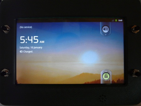
Android default lock screen
Moreover, you'll have immediate access to the Android shell, so you can use the shell commands to interact with the system and see the output messages on the console. Using the serial console doesn't prevent you from using also the adb tool to access the system.
- connect the system to Ethernet LAN (RJ45 connector, J6)
- connect a 12Vcc power supply to to the power jack (JP2)
Once power has been applied, the system will boot loading the software components from the internal flash. Once the boot process has completed, you'll get the default Android "desktop":
You can now access the system using adb.
Running the Android Debug Bridge (ADB)[edit | edit source]
ADB is a fundamental development tool and enables remote access to the Android device. ADB is provided with the Android SDK, so before using it you must install the SDK.
To establish the ADB connection, on a Linux host machine launch the following commands:
$ export PATH=${PATH}:<your_sdk_dir>/platform-tools
$ export ADBHOST=<target's ip address>
$ adb kill-server
$ adb start-server
To check the connection, please launch
$ adb devices
If everything is working properly, you should see the following messages:
$ adb devices
List of devices attached
emulator-5554    device
You can open a remote shell using the following command:
$ adb shell
To install an application (in .apk format), you can use the following commmand:
$ adb install <path to apk>

