AURA SOM/AURA Evaluation Kit/pdf
Getting started[edit | edit source]
Kit Identification Codes[edit | edit source]
The development kits are identified by a couple of codes:
- P/N Part Number identification code
- S/N Serial Number identification code
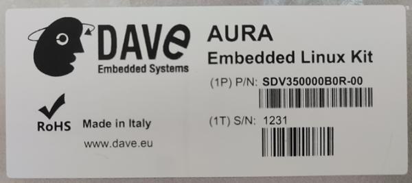
These codes are printed on a label stuck to the box containing the kit.
For example, the following picture shows such a label of an AURA Evaluation Kit with Serial Number 1231
These codes are required to complete the registration process of the kit.
Unboxing[edit | edit source]
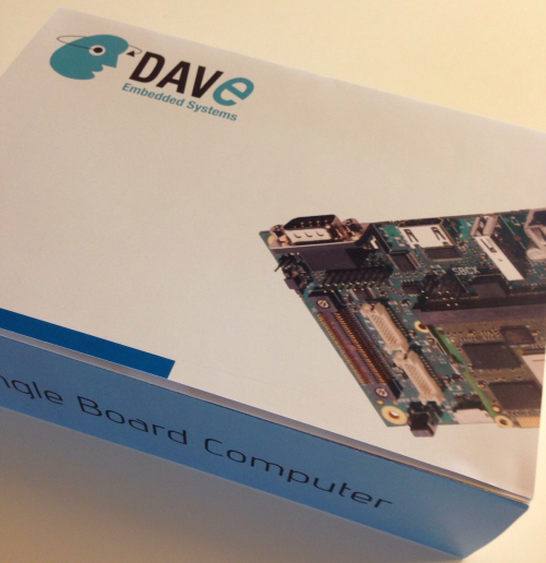
Once you've received the kit, please open the box and check the kit contents with the packing list included in the box, using the table on this chapter as a reference.
The hardware components (SOM, carrier boards and display) are pre-assembled, as shown in the picture below:
Video[edit | edit source]
Kit Contents[edit | edit source]
The following table list the kit components:
| Component | Description |
|---|---|
| SBCX with AURA SOM | |
| AM-800480BTMQW-TG4H 7” 800x480 LCD display LVDS interface with capacitive touchscreen | |
| M.2 Wifi module with M.2 adapter | |
| AC/DC Single Output Wall Mount adapter Output: +12V – 2.0 A | |
| FTDI USB/RS232 cable adapter
FTDI code: CHIPI-X10 | |
| DB9 Male Serial port adapter | |
| MicroSDHC card |
Order codes[edit | edit source]
| Order code | Description |
|---|---|
| SDV3500000B1R-00 | This code refers to the default configuration detailed above |
microSD Layout[edit | edit source]
The microSD provided with the kit is used to store:
- a bootable partition (mmcblk0p1, vfat) containing:
- binary images (u-boot and kernel images)
- root file system partition (mmcblk0p2, ext4)
Connections[edit | edit source]
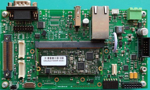
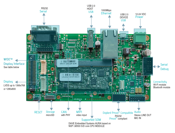
This section describes how to quickly start the Evaluation Kit. The picture below shows the AURA SOM inserted into the Evaluation Kit:
The system is programmed to automatically boot Linux at power up, loading the bootloader, the kernel and device tree image and the root file system from the SD card memory.
To connect to the system:
- connect the 12Vcc power supply to JP2 on the board
- connect the DB9 adapter bracket to the J22 connector on the SBCX and connect the DB9 connector to the PC COM port through a NULL-modem cable (not provided)
- start your favorite terminal emulator software on PC (eg: PuTTY, Minicom, ...); communication parameters are 115200,N,8,1
- (optional) connect the ethernet cable from your LAN hub/switch to the J16 RJ45 connector
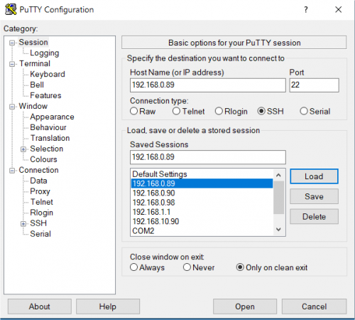
- start SSH, using the following parameters:
- ip address: 192.168.0.89
- username: root
- empty password
- start SSH, using the following parameters:
First boot[edit | edit source]
Once power has been applied, U-Boot bootloader will be executed and the debug messages will be printed on the serial console. U-Boot automatically runs the autoboot macro, that loads the kernel/dtb and launches it with the options for mounting the root file system from the SD card.
At the end of the boot process, a demo application is launched and you can interact with the system using the touchscreen. The Linux shell is available on the serial console. Moreover, both telnet and ssh services are available to connect to the system through the network.
Serial console[edit | edit source]
A simple Windows serial and SSH/telnet client and terminal can be downloaded from here.
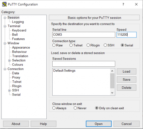
The following picture shows the serial setup for connecting to the EVK:
once selected the COM[x] serial port, click the Open button which starts the terminal. Once powered, the EVK shows the U-boot debug messages printed on the serial console.
Connecting through SSH[edit | edit source]
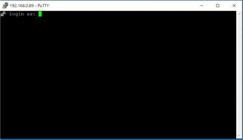
The following picture shows the SSH connection to the EVK:
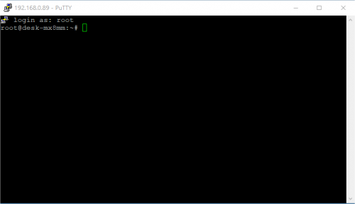
once selected the IP address, click the Open button which starts the terminal. Once connected, the EVK shows the linux kernel prompt login for inserting the login:
Then use the root login username without password:
Boot Configurations[edit | edit source]
AURA Evaluation Board is built upon i.MX93x family processor.
The following sections detail boot configuration options, which differ depending on the SoM.
For more information about AURA boot options, see the related page on AURA Hardware Manual.
Available options[edit | edit source]
Boot modes can be selected by J32 jumper switches which act directly on J2.20 BOOT_MODE_SEL SOM pin.
| Boot options order code | Jumper mounted | Jumper not mounted |
|---|---|---|
| Boot from eMMC | SD | eMMC |
Reset Button[edit | edit source]
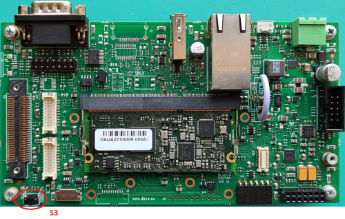
AURA Evaluation Board has a pushbutton directly connected to the PMIC_ON_REQ signal which drives a SOM hardware reset.
S3 is the hardware reset button.
General Information[edit | edit source]
Product Highlights[edit | edit source]
The AURA Evaluation Kit platform presented here provides a compact solution for any industry and can be easily interfaced with Plant Automation Control thanks to IEC-61131 SW language environment and/or other plug-ins like QT framework or multimedia GStreamer video applications.
The following table summarizes the main hardware and software features available with AURA Evaluation Kit:
Hardware[edit | edit source]
| Subsystem | Characteristics |
|---|---|
| CPU | NXP i.MX93 Single/Dual core |
| USB | Host and device |
| Serial Ports | RS232/422/485 multiprotocol LVTTL UART CAN interface |
| Ethernet | 10/100/1000Mbps WIDE TM interface with second ethernet RGMII port signals |
| Display | LVDS interface |
| Video | MIPI (optional) interfaces |
| Touchscreen | Capacitive |
| Audio | Stereo OUT and MIC in (on 2x2.54mm connector) |
| Connectivity | Bluetooth and Wi-Fi |
| PSU | 12 to 24V DC |
| Mechanical Dimensions | 85x156mm - Standard DIN (9 modules) |
Software[edit | edit source]
| Subsystem | Options |
|---|---|
| Operating System | Linux, Android |
| Distribution | Yocto, Debian, Buildroot |
| Graphical Framework | Qt |
| Applications | SoftPLC, IoT runtime, nodeJS |
Block diagram[edit | edit source]
The following picture shows a simplified block diagram of the AURA SOM Evaluation kit.
Main functional subsystems and interfaces are depicted.
The heart of the Evaluation Kit is the AURA SOM module: please refer to the following Product Highlights page for the Evaluation Kit product highlights information.
Here below a summary for the main characteristics of the Kit.
Features Summary[edit | edit source]
| Feature | Specifications |
|---|---|
| CPU | NXP i.MX93 |
| Serial Ports | 1x UART RS232 1x LVTTL UART 1x UART RS232 on pin strip (debug port) 1x CAN interface |
| Ethernet | 10/100/1000Mbps |
| Display | LVDS |
| Camera | MIPI Video input (optional) |
| Storage | microSD slot |
| USB | 1x USB 2.0 Host port 1x USB 2.0 OTG port |
| Audio | TLV320AIC310 codec |
| Connectivity | BT and Wi-Fi M.2 module |
| Miscellaneous | Capacitive touch controller 40 GPIOs (on WIDE connector) JTAG (wired optionally) Additional ECSPI, UART, I2C, SDIO on WIDE™ connector |
Electrical, Mechanical and Environmental Specifications[edit | edit source]
| Electrical / Mechanicals | Specifications |
|---|---|
| Supply voltage | + [12 - 24] V |
| Dimensions | 156 mm x 84 mm |
| Weight | 107,6 g |
| Operating Temperature | 0..70 °C |
Interfaces and Connectors[edit | edit source]
CPU connector[edit | edit source]
Description[edit | edit source]
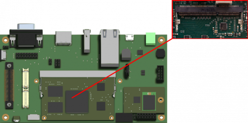
J10 is the 204-pins SODIMM mating connector for the AURA SOM.
For a detailed description of the SOM pinout, please refer to the AURA Hardware Manual.
JTAG[edit | edit source]
Description[edit | edit source]
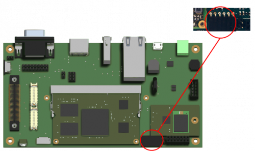
JTAG signals are routed to J34 a 20x2x1.00 mm One Piece Interface dedicated to the MIPI camera input too.
Signals[edit | edit source]
The following table describes the JTAG interface signals on J34 connector:
| Pin# | SOM Pin# | Pin name | Pin function | Pin Notes |
|---|---|---|---|---|
| 1 | - | 5V_IN | ||
| 10 | J1.92 | PCIE_RXN | JTAG_TDI | |
| 12 | J1.94 | PCIE_RXP | JTAG_TMS | |
| 14 | J1.96 | PCIE_TXN | JTAG_TCK | |
| 16 | J1.96 | PCIE_TXP | JTAG_TDO | |
| 5, 8, 11, 14, 17, 23, 24, 29, 30, 35, 36 |
- | DGND | Ground | |
| 20 | - | 3V3 |
Ethernet[edit | edit source]
Description[edit | edit source]
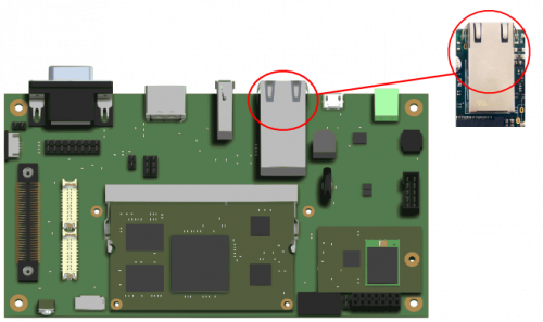
J16 is a standard RJ45 connectors connected to the SOM integrated ethernet controller and PHY.
Signals[edit | edit source]
The following table describes the interface signals:
| Pin# | SOM Pin# | Pin name | Pin function | Pin Notes |
|---|---|---|---|---|
| 11 | J10.19 | ETH0_TXRX0_P | Transmit and receive pair 0 data + | |
| 10 | J10.21 | ETH0_TXRX0_M | Transmit and receive pair 0 data - | |
| 4 | J10.23 | ETH0_TXRX1_P | Transmit and receive pair 1 data + | |
| 3 | J10.27 | ETH0_TXRX2_P | Transmit and receive pair 2 data + | |
| 2 | J10.29 | ETH0_TXRX2_M | Transmit and receive pair 2 data - | |
| 5 | J10.25 | ETH0_TXRX1_M | Transmit and receive pair 1 data - | |
| 8 | J10.31 | ETH0_TXRX3_P | Transmit and receive pair 3 data + | |
| 9 | J10.33 | ETH0_TXRX3_M | Transmit and receive pair 3 data - | |
| 17 | J10.15 | 3V3_ETH1_LED2 | Eth link led | |
| 20 | J10.13 | 3V3_ETH1_LED1 | Eth activity led |
Device mapping[edit | edit source]
The network interface mapped at eth0 device in Linux.
Device usage[edit | edit source]
The peripheral is used the standard kernel interface and network protocol stack.
Console interface[edit | edit source]
Description[edit | edit source]
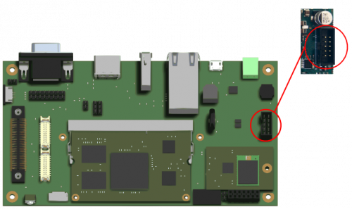
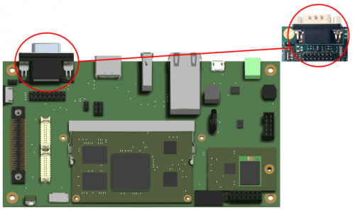
The Console interface is available on the Evaluation Kit at the connector J22.
J22 is a 10 pin (5x2x2.54mm) header connector for the RS232 two-wires UART2 port, used for debug purposes (bootloader and operating system serial console).
Signals[edit | edit source]
The following table describes the interface signals:
| Pin# | SOM Pin# | Pin name | Pin function | Pin Notes |
|---|---|---|---|---|
| 1,2,4,6,,7,8,10 | - | N.A. | N.C. | Not connected |
| 3 | J10.189 | RS232_RX | Receive line | |
| 3 | J10.187 | RS232_TX | Transmit line | |
| 9 | - | DGND | Ground |
Device mapping[edit | edit source]
LPUART1 is mapped to /dev/ttyLP0 device in Linux. The peripheral is used as the default serial console, both for the bootloader and the kernel.
Device usage[edit | edit source]
To connect to the debug serial port:
- connect the DB9 adapter bracket to the J22 connector on the SBCX board
- connect a serial cable between DB9 connector and PC COM port through a NULL-modem cable (not provided)
- start your favorite terminal emulator software on PC (eg: PuTTY); communication parameters are: 115200,N,8,1
UARTs interface[edit | edit source]
Description[edit | edit source]
The UARTs interface available on the Evaluation Kit are mapped to the following connectors:
- J21 is a standard DB9 male connector for the configurable UART2 port. The board provides some configuration options for the selection of the UART mode (RS232 at 2 or 4 wires)
- J25 is a 6x1x2.54mm horizontal socket header for the UART4 port. This is a Digilent Pmod™ Compatible connector for the UART Pmod™ Compatiblemodule (6-Pin Pmod™ Compatible Connector Digilent Pmod™ Interface Specification Type 4 UART)
Signals[edit | edit source]
The following tables describes the interface signals
UART2[edit | edit source]
|
In the schematics page 13, the signals label are referring to the original AXEL Lite EVK SOM's signals. UART5 is referencing the AXEL Lite UART connection and should be used just as a signal labels. |
| Pin# | SOM Pin# | Pin name | RS-232 |
|---|---|---|---|
| 1 | - | Not connected | Not connected |
| 2 | J10.95 | UART5_A | UART2 receive line |
| 3 | J10.93 | UART5_Y | UART2 transmit line |
| 4 | - | Not connected | Not connected |
| 5 | - | DGND | Ground |
| 6 | - | Not connected | Not connected |
| 7 | J10.105 | UART5_Z | UART2 Request To Send |
| 8 | J10.107 | UART5_B | UART2 Clear To Send |
| 9 | - | Not connected | Not connected |
UART4[edit | edit source]
| Pin# | SOM Pin# | Pin name | Pin function | Pin Notes |
|---|---|---|---|---|
| 1 | J10.50 | PMOD_A0 | Clear to send | |
| 2 | J10.89 | PMOD_A1 | Transmit data | |
| 3 | J10.91 | PMOD_A2 | Receive data | |
| 4 | J10.40 | PMOD_A3 | Request to send | |
| 5 | - | DGND | Ground | |
| 6 | - | 3V3 | +3.3 V |
Device mapping[edit | edit source]
- UART2 is mapped to
/dev/ttyLP1device in Linux - UART4 is mapped to
/dev/ttyLP3device in Linux
Device usage[edit | edit source]
- UART2 is MultiProtocol supporting the RS232 protocol
- UART4 can be used with a PMOD adapter or with a TTL peripheral
micro SD interface[edit | edit source]
Description[edit | edit source]
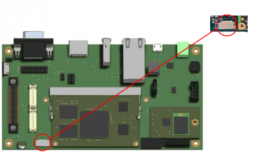
The micro SD interface available on the Evaluation Kit at the connector J26.
J26 is a Micro-SD card header. This interface is connected to the USDHC2 controller of the i.MX93x CPU.
Signals[edit | edit source]
The following table describes the interface signals:
| Pin# | SOM Pin# | Pin name | Pin function | Pin Notes |
|---|---|---|---|---|
| 1 | J10.79 | SD_DAT2 | Data 2 | |
| 2 | J10.81 | SD_DAT3 | Data 3 | |
| 3 | J10.83 | SD_CMD | CMD | |
| 4 | - | 3V3 | +3.3 V | |
| 5 | J10.85 | SD_CLK | Clock | |
| 6, 12 | - | DGND | Ground | |
| 7 | J10.75 | SD_DAT0 | Data 0 | |
| 8 | J10.77 | SD_DAT1 | Data 1 | |
| 9, 10, 11 | - | SD_SHIELD | Shield | |
| 13 | J10.177 | CD | Card detect | SD2_CD_B on i.MX93x |
Device mapping[edit | edit source]
The microSD card is mapped to /dev/mmcblk1. The available partitions are shown as /dev/mmcblk1p1, /dev/mmcblk1p2, etc.
Device usage[edit | edit source]
The device can be mounted/accessed as a standard block device in Linux.
USB ports[edit | edit source]
Description[edit | edit source]
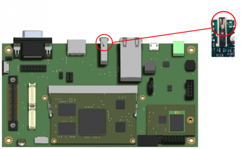
AURA Evaluation Kit provides two USB ports, one Host and one OTG:
- J17 is a standard USB Host 2.0 Type A connector
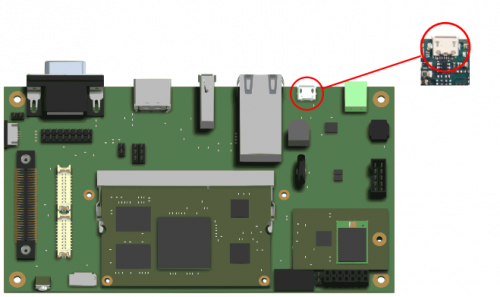
- J18 is a micro-AB type receptacle for a USB OTG connection: this interface can operate (optionally) in Host mode and Device (peripheral) mode
Signals[edit | edit source]
The following table describes the interface signals
USB Host[edit | edit source]
| Pin# | SOM Pin# | Pin name | Pin function | Pin Notes |
|---|---|---|---|---|
| 1 | J10.188 | USB_HOST_VBUS | VBUS | USB2_VBUS |
| 2 | J10.202 | USB_HOST_DN | USB Host Data - | USB2 D_N |
| 3 | J10.200 | USB_HOST_DP | USB Host Data + | USB2 D_P |
| 4 | - | DGND | Ground |
USB OTG[edit | edit source]
| Pin# | SOM Pin# | Pin name | Pin function | Pin Notes |
|---|---|---|---|---|
| 6, 7, 8, 9 | - | USB_OTG_SH Shield | ||
| 1 | J10.186 | USB_OTG_VBUS | VBUS | USB1_VBUS |
| 2 | J10.196 | USB_OTG_DN | USB OTG Data - | USB1 D_N |
| 3 | J10.198 | USB_OTG_DP | USB OTG Data + | USB1 D_P |
| 4 | J10.192 | ENET_RX_ER | USB OTG ID | USB1_ID |
| 5 | - | GND | Ground |
Device usage[edit | edit source]
The USB Host port, connected to the USB2_OTG i.MX93x port, can be used under Linux for connecting USB peripheral devices: the related peripheral driver has to be integrated into the Linux kernel.
The USB OTG port, connected to the USB1_OTG i.MX93x port, can be easily tested using the Mass Storage Gadget driver.
LVDS[edit | edit source]
Description[edit | edit source]
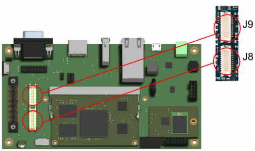
SBC AXEL provides two LVDS interfaces, LVDS0 and LVDS1. AURA SOM supports one LVDS channel on J8 Hirose (cod. DF13A-20DP-1.25V) double row 1.25mm pitch miniature crimping connector.
Signals[edit | edit source]
The following tables describes the interface signals
LVDS0[edit | edit source]
| Pin# | SOM Pin# | Pin name | Pin function | Pin Notes |
|---|---|---|---|---|
| 1, 2 | - | 3.3V_LCD0 | 3.3 V | |
| 3, 4, 7, 10,
13, 16, 19 |
- | DGND | Ground | |
| 5 | J10.137 | LVDS0_TX0_N | LVDS Data 0 - | |
| 6 | J10.139 | LVDS0_TX0_P | LVDS Data 0 + | |
| 8 | J10.141 | LVDS0_TX1_N | LVDS Data 1 - | |
| 9 | J10.143 | LVDS0_TX1_P | LVDS Data 1 + | |
| 11 | J10.145 | LVDS0_TX2_N | LVDS Data 2 - | |
| 12 | J10.147 | LVDS0_TX2_P | LVDS Data 2 + | |
| 14 | J10.133 | LVDS0_CLK_N | LVDS Clock - | |
| 15 | J10.135 | LVDS0_CLK_P | LVDS Clock + | |
| 17 | J10.149 | LVDS0_P17 | LVDS Data 3 - | |
| 18 | J10.151 | LVDS0_P18 | LVDS Data 3 + | |
| 20 | J10.46 | LVDS0_P20 | TPM3.CH3 |
Device mapping[edit | edit source]
LVDS is mapped to LVDS-1 DRM "connector": see DESK-MX9-L LVDS peripheral.
Power sequence[edit | edit source]
Most of the LCD panels have many supplies and need a specific timing to power the rails and start the signals.
The Evaluation Kit provides GPIO controlled power rails that can be leveraged both at bootloader and kernel level to meet any specifications.
The following sections describe the available rails:
3V3_LCD[edit | edit source]
The most common voltage to supply the LCD panel internal rail 3V3_LCD0 is enabled by GPIO1_IO10
5V_LCD[edit | edit source]
The most common voltage to supply the LCD panel backlight rail 5V_LCD0 is enabled by GPIO2_IO24
Device usage[edit | edit source]
The associated framebuffer device is accessed in Linux through the standard graphic access.
Touchscreen interface[edit | edit source]
Description[edit | edit source]
The Evaluation Kit default LCD panel interfaces the touchscreen via USB, thus it is connected to J17, see USB port section.
Many touchscreen types use instead an I2C interface with two additional control signals (RST, IRQ). To use these type of touchscreens the interface signals can be routed to the expansion connector J33.
An external circuit is recommended to correctly condition the interface signals, such as buffers and pull up/down, according to the touchscreen specifications.
Signals[edit | edit source]
The following table describes the available I2C signals on J33 connector, see GPIO section for available control signals:
| Pin# | SOM Pin# | Pin name | Pin function | Pin Notes |
|---|---|---|---|---|
| 18 | J10.38 | GPIO2_IO29 | I2C3_SCL | |
| 20 | J10.48 | GPIO2_IO28 | I2C3_SDA | |
| 48, 50 | - | 3V3 | +3.3V | BOARD_PGOOD driven rail |
| 56, 58 | - | VIN | Always powered | |
| 2, 16, 22, 36, 46, 59, 60 | - | DGND | Ground |
All the I2C signals use 0 - 3.3V levels, external pull-ups to 3V3_CB are needed.
Device mapping[edit | edit source]
The device is typically mapped to /dev/touchscreen0 device in Linux.
The touch controller is attached to the generic Linux input event interface (evdev).
For I2C touchscreen controllers a dedicated node in the device-tree has to be configured to correctly bind the driver.
Device usage[edit | edit source]
The touchscreen device is often passed as parameter to the user interface application or is automatically discovered.
Touchscreen can be tested with the evtest tool that prints the finger coordinates to the console.
MIPI[edit | edit source]
Description[edit | edit source]
J34 is a 20x2x1.00 mm One Piece Interface dedicated to the MIPI camera input.
This connector can be used as a Camera Interface for connecting a MIPI CSI-2 camera device.
Signals[edit | edit source]
The following table describes the interface signals:
| Pin# | SOM Pin# | Pin name | Pin function | Pin Notes |
|---|---|---|---|---|
| 1 | - | 5V_IN | ||
| 3 | J10.97 | AUX_PWR_EN | connected to GPIO3_IO19 | |
| 13 | - | AUX_USB_DN | ||
| 15 | - | AUX_USB_DP | ||
| 19 | J10.53 | CAM_PWD | connected to GPIO1_IO11 | |
| 20 | - | 3V3 | ||
| 21 | J10.51 | CAM_RSTn | Not connected | |
| 22 | J10.60 | CAM_CLK | Not connected | |
| 25 | J10.102 | CSI_CLK0M_1 | ||
| 26 | J10.48 | CSI_SDA | I2C3_SDA | |
| 27 | J10.104 | CSI_CLK0P_1 | ||
| 28 | J10.38 | CSI_SCL | I2C3_SCL | |
| 31 | J10.110 | CSI_D1M_1 | ||
| 32 | J10.106 | CSI_D0M_1 | ||
| 33 | J10.112 | CSI_D1P_1 | ||
| 34 | J10.108 | CSI_D0P_1 | ||
| 37 | J10.118 | CSI_D3M_1 | Not connected | |
| 38 | J10.114 | CSI_D2M_1 | Not connected | |
| 39 | J10.120 | CSI_D3P_1 | Not connected | |
| 40 | J10.116 | CSI_D2P_1 | Not connected | |
| 5, 8, 11, 14, 17, 23, 24, 29, 30, 35, 36 |
- | DGND | Ground |
Device mapping[edit | edit source]
The MIPI CSI peripheral is mapped to the corresponding /dev/video<X> device in Linux. The device mapping depends on the device tree configuration.
Audio[edit | edit source]
Description[edit | edit source]
The Audio interface available on the Evaluation Kit at the connector J27.
J27 is a 7x2x2.54mm header. The audio codec is a TLV320AIC3100 device connected to the I²S interface.
Signals[edit | edit source]
The following table describes the interface signals:
| Pin# | Pin name | Pin function | Pin Notes |
|---|---|---|---|
| 4, 5, 8, 9 | AGNDM Analog | Ground | |
| 1 | AUX_RES | Analog ground | |
| 2 | AUXR | Microphone in right | |
| 3 | AUXL | Microphone in left | |
| 6 | SPKM | Speaker out (negative) | |
| 7 | SPKP | Speaker out (positive) | |
| 10 | HSOR | Audio Headset right | |
| 11 | HSOL | Audio Headset left | |
| 12 | MIC_BIAS | Microphone bias | |
| 13 | AUD_HP_VGND | Analog ground |
Device mapping[edit | edit source]
The Audio interface is mapped to card0 ALSA device in Linux. The ALSA peripheral #0: SBCX_TLV320 can be accessed via alsa-utils with hardware address 0.
Device usage[edit | edit source]
For example, it is possible to play a file using aplay
RTC[edit | edit source]
Description[edit | edit source]
i.MX93 integrates a Secure real-time clock (RTC) powered by the Battery Backed Security Module (BBSM). The BBSM is in the low power section in the battery backed by the VBAT (or RTC) power domain. This enables it to keep this data valid.
AURA SOM uses the internal RTC device provided by i.MX93 SoC. The RTC stays powered on BBSM mode. The BBSM mode keeps RTC and BBSM logic alive: only the power for the BBSM domain remains on. More info in the i.MX93 datasheet.
The RTC keeps the date while the VIN power supply stays on. A proper power mode has to be configured for low power consumption.
Device mapping[edit | edit source]
Internal RTC device is mapped to /dev/rtc0 device in Linux.
Device usage[edit | edit source]
The peripheral can be accessed through the date and hwclock linux commands.
Wi-Fi/BT[edit | edit source]
The Wi-Fi and BT socket interface supports a WiFi add-on providing WiFi 802.11 bgn and Bluetooth connectivity.
Description[edit | edit source]
This interface is available on the Evaluation Kit at the connector J2.
J2 is a 30-pin 0.50mm Pitch SlimStack™ Receptacle. This connector is dedicated to the WiFi add-on module.
Signals[edit | edit source]
The following table describes the interface signals:
| Pin# | SOM Pin# | Pin name | Pin function | Pin Notes |
|---|---|---|---|---|
| 1, 2 | - | 5V | Power supply | |
| 3, 4 | - | 3.3V | Power supply | |
| 5, 6, 9, 10, 19 | - | DGND | Ground | |
| 7 | J15.18 | MMC2_CMD | ||
| 8 | J15.16 | MMC2_CLK | ||
| 11 | J15.20 | MMC2_DAT0 | ||
| 13 | J15.22 | MMC2_DAT1 | ||
| 15 | J15.24 | MMC2_DAT2 | ||
| 17 | J15.26 | MMC2_DAT3 | ||
| 21 | J15.114 | UART_RX | Used only for BT peripheral | |
| 23 | J15.110 | UART_CTS | Used only for BT peripheral | |
| 24 | J15.36 | BT_F5 | Used only for BT peripheral | |
| 25 | J15.114 | UART_TX | Used only for BT peripheral | |
| 26 | J15.38 | BT_F2 | Used only for BT peripheral | |
| 27 | J15.116 | UART_RTS | Used only for BT peripheral | |
| 28 | J15.56 | IRQ | ||
| 29 | J15.34 | BT_EN | Used only for BT peripheral | |
| 30 | J15.32 | WIFI_EN | ||
| 12, 14, 16, 18, 20, 22 | - | N.C. | Not connected |
WiFi[edit | edit source]
Device mapping[edit | edit source]
The WiFi peripheral is mapped to the corresponding mlan0 device in Linux. The network peripheral is visible under the ifconfig network configuration utility.
Device usage[edit | edit source]
The peripheral is used the standard kernel interface and network protocol stack.
Bluetooth[edit | edit source]
Device mapping[edit | edit source]
The BT peripheral is mapped to the /dev/ttymxc2 serial port in Linux. It can be mounted as an hci device with the hci tools commands.
Device usage[edit | edit source]
The peripheral is used by the standard kernel interface and BlueZ protocol stack.
GPIOs[edit | edit source]
Description[edit | edit source]
i.MX93 can handle external pins in many different ways and most of them can be configured as GPIOs. When a pin is set as a GPIO, it is possible to read its value, change its direction or change output value directly from the shell.
Signals[edit | edit source]
The following table describes some GPIOs signals available on J33 WIDE™ connector:
| Pin# | SOM Pin# | Pin name | GPIO index | Alternate function |
|---|---|---|---|---|
| 1 | J10.134 | SD1_STROBE | GPIO3_IO018 | SD1_STROBE |
| 2 | J10.179 | GPIO_IO00 | GPIO2_IO30 | SPI6_PCS0 |
| 3 | J10.136 | - | - | - |
| 4 | J10.181 | GPIO_IO03 | GPIO2_IO3 | SPI6_SCK |
| 5 | J10.138 | SD1_DATA0 | GPIO2_IO2 | SD1_DATA0 |
| 6 | J10.183 | GPIO_IO01 | GPIO2_IO01 | SPI6_SIN |
| 7 | J10.140 | SD1_DATA1 | GPIO2_IO3 | SD1_DATA1 |
| 8 | J10.195 | GPIO_IO13 | GPIO2_IO13 | SPI6_SOUT |
| 9 | J10.142 | SD1_DATA2 | GPIO2_IO4 | SD1_DATA2 |
| 11 | J10.144 | SD1_DATA3 | GPIO2_IO5 | SD1_DATA3 |
| 13 | J10.148 | SD1_DATA4 | GPIO2_IO6 | SD1_DATA4 |
| 15 | J10.150 | SD1_DATA5 | GPIO2_IO7 | SD1_DATA5 |
| 17 | J10.152 | SD1_DATA6 | GPIO2_IO8 | SD1_DATA6 |
| 18 | J10.38 | GPIO2_IO29 | GPIO5_IO18 | I2C3_SCL |
| 19 | J10.154 | SD1_DATA7 | GPIO2_IO9 | SD1_DATA7 |
| 20 | J10.48 | GPIO2_IO28 | GPIO5_IO19 | I2C3_SDA |
| 21 | J10.156 | ENET2_TD3 | GPIO4_IO16 | ENET1_RGMII_TD3 |
| 23 | J10.158 | ENET2_TD2 | GPIO4_IO17 | ENET1_RGMII_TD2 |
| 24 | J10.46 | GPIO_IO24 | GPIO2_IO24 | |
| 25 | J10.160 | ENET2_TD1 | GPIO4_IO18 | ENET1_RGMII_TD1 |
| 26 | J10.28 | WDOG_ANY | GPIO1_IO15 | - |
| 27 | J10.162 | ENET2_TD0 | GPIO4_IO19 | ENET1_RGMII_TD30
UART4_TX |
| 28 | J10.191 | GPIO_IO12 | GPIO2_IO12 | I2C8_SDA |
| 29 | J10.166 | ENET2_TXC | GPIO4_IO21 | ENET1_RGMI_TXC |
| 30 | J10.193 | GPIO_IO13 | GPIO2_IO13 | I2C8_SCL |
| 31 | J10.168 | ENET2_TX_CTL | GPIO4_IO220 | ENET1_RGMI_TX_CTL
UART4_DTR |
| 32 | J10.50 | CCM_CLK01 | GPIO3_IO26 | |
| 33 | J10.170 | ENET2_MDC | GPIO4_IO14 | ENET1_MDC
UART4_DCR |
| 34 | J10.40 | GPIO_IO07 | GPIO2_IO07 | |
| 35 | J10.172 | ENET2_MDIO | GPIO4_IO15 | ENET1_MDIO
UART4_RIN |
| 37 | J10.174 | ENET2_RX_CTL | GPIO4_IO22 | ENET1_RGMII_RX_CTL
UART4_DSR |
| 39 | J10.176 | ENET2_RD0 | GPIO4_IO24 | ENET1_RGMII_RD0
UART4_RX |
| 41 | J10.178 | ENET2_RD1 | GPIO4_IO25 | ENET1_RGMII_RD1 |
| 43 | J10.180 | ENET2_RD2 | GPIO4_IO26 | ENET1_RGMII_RD2
UART4_CTS |
| 45 | J10.182 | ENET2_RD3 | GPIO4_IO27 | ENET1_RGMII_RD3 |
| 47 | J10.184 | ENET2_RXC | GPIO4_IO23 | ENET1_RGMI_RXC |
| 49 | J10.124 | ENET1_MDC | GPIO4_IO00 | I3C2_SCL |
| 51 | J10.126 | ENET1_MDIO | GPIO4_IO01 | I3C2_SDA |
| 53 | J10.128 | SD1_CLK | GPIO3_IO08 | SD1_CLK |
| 55 | J10.130 | SD1_CMD | GPIO3_IO09 | SD1_CMD |
| 57 | J10.132 | ETH1_LED5 | - | - |
Device mapping[edit | edit source]
GPIOs can be used directly on Linux kernel device driver or can be configured on the device tree.
Device usage[edit | edit source]
See the GPIOs page on the DESK-MX9-L Software Manual.
Electrical and Mechanical Documents[edit | edit source]
Schematics[edit | edit source]
Please find here below the links for the AURA Evaluation Kit schematics and the related documents (BOM and layout):
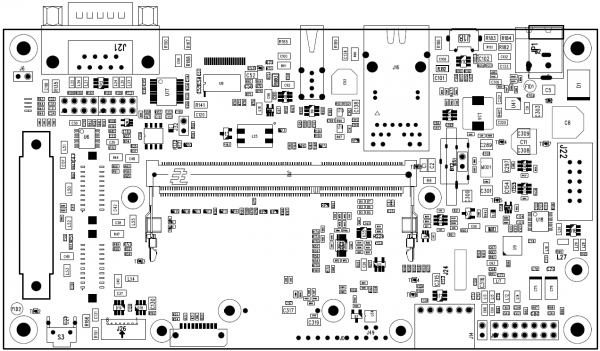
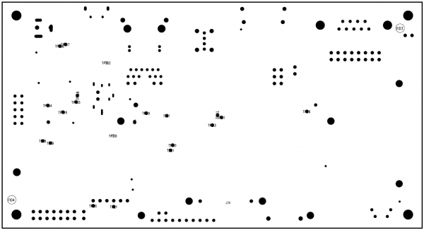
Layout[edit | edit source]
Mechanical specifications[edit | edit source]
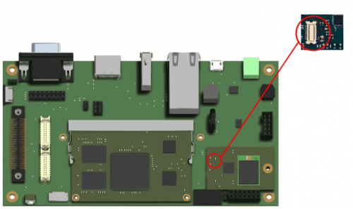
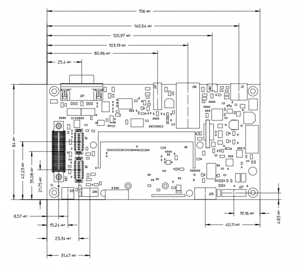
This page describes the mechanical characteristics of the AURA EVK carrier board.
Board layout[edit | edit source]
Dimensions[edit | edit source]
3D drawings[edit | edit source]
Mechanical data[edit | edit source]
| Dimension | Value |
|---|---|
| Width | 156 mm |
| Depth | 84 mm |
| Max component's height (top) | 13.87 mm |
| Max component's height (bottom) | |
| PCB height | 1.69 mm |
