MITO 8M SOM/MITO 8M Hardware/pdf
General Information[edit | edit source]
MITO 8M SOM Block Diagram[edit | edit source]
[[File:Mito-bd-1.0.0-300dpi.png|thumb|MITO 8M Block diagram|none]]
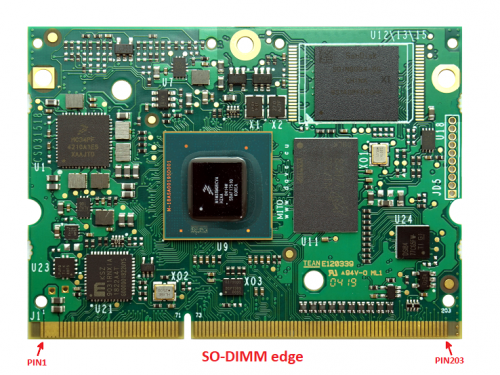
MITO 8M SOM TOP View[edit | edit source]
[[File:DMI-Mito-top.png|thumb|MITO 8M TOP View|none]]
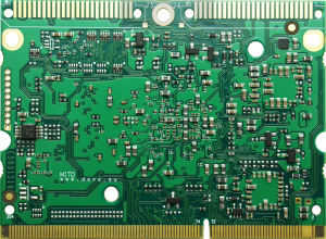
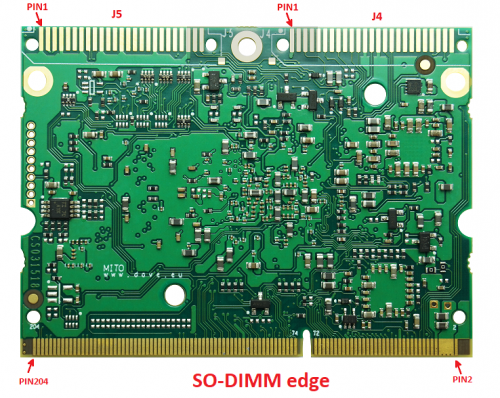
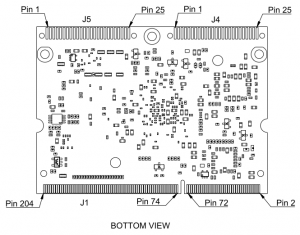
MITO 8M SOM BOTTOM View[edit | edit source]
Processor and memory subsystem[edit | edit source]
The heart of MITO 8M module is composed by the following components:
- i.MX8M SoC application processor
- Power supply unit
- LPDDR4 memory bank
- eMMC or NAND flash banks
- Connectors:
- 1 x 204 pins SO-DIMM edge connector with interfaces signals
- partially compatible with AXEL Lite SOM
- 2 x 25 pins One Piece mating board layout Expansion
- 1 x 204 pins SO-DIMM edge connector with interfaces signals
This chapter shortly describes the main MITO 8M components.
Processor Info[edit | edit source]
| Processor | i.MX8M Dual | i.MX8M Quad |
| # Cores | 2x Arm® Cortex®-A53
1x Arm® Cortex®-M4 |
4x Arm® Cortex®-A53
1x Arm® Cortex®-M4 |
| Clock | 1.3 GHz
1.5 GHz | |
| L2
Cache |
1 MB | |
| LPDDR4 | 32 bit @ 1600 MHz
(LPDDR4-3200) | |
| GPU | 4 Shader
OpenGL ES 1.1, 2.0, 3.0, 3.1 Open CL 1.2 Vulkan | |
| VPU | 4Kp60 HEVC/H.265 main, and main 10 decoder
4Kp60 VP9 decoder 4Kp30 AVC/H.264 decoder 1080p60 MPEG-2, MPEG-4p2, VC-1, VP8, RV9, AVS, MJPEG, H.263 decoder | |
| Display
Controller |
Dual Independent
Display Support up tp 4kp60 | |
| Video
Output |
1x HDMI 2.0a
1x MIPI-DSI (with MIPI to LVDS bridge) | |
| Camera
Input |
2x MIPI CSI
(4-lanes each) | |
| PCIe | 2x PCIe 2.0
(1-lane each) | |
| USB | 2x USB 3.0
Dual role | |
RAM memory bank[edit | edit source]
LPDD4 SDRAM memory bank is composed by 1x 32-bit width chip. The following table reports the SDRAM specifications:
| CPU connection | Multi-mode DDR controller (MMDC) |
| Size max | 4 GB |
| Width | 32 bit |
| Speed | 1600 MHz |
eMMC flash bank[edit | edit source]
On board main storage memory eMMC is connected to the SDIO1 interface and it can act as boot peripheral. The following table reports the eMMC flash specifications:
| CPU connection | SDIO1 |
| Size min | 4 GB |
| Size max | 64 GB |
| Bootable | Yes |
NAND flash bank[edit | edit source]
| Section not completed yet |
Alternative option for main storage memory can be a 8-bit wide NAND flash connected to the CPU's Raw NAND flash controller. It can act as boot peripheral. The following table reports the NAND flash specifications:
| CPU connection | Raw NAND flash controller |
| Page size | TBD |
| Size min | TBD |
| Size max | TBD |
| Width | 8 bit |
| Chip select | TBD |
| Bootable | Yes |
Memory map[edit | edit source]
For detailed information, please refer to chapter 2 “Memory Maps” of the i.MX8M Applications Processor Reference Manual
Power supply unit[edit | edit source]
MITO 8M embeds all the elements required for powering the unit, therefore power sequencing is self-contained and simplified. Nevertheless, power must be provided from carrier board, and therefore users should be aware of the ranges power supply can assume as well as all other parameters.
Hardware versioning and tracking[edit | edit source]
MITO 8M SOM implements well established versioning and tracking mechanisms:
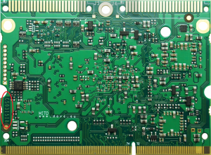
- PCB version is copper printed on PCB itself, as shown in Fig. 1
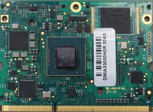
- serial number: it is printed on a white label, as shown in Fig. 2: see also Product serial number page for more details
- ConfigID: it is used by software running on the board for the identification of the product model/hardware configuration. For more details, please refer to this link
- On MITO 8M SOM ConfigID is stored on OTP memory
MITO 8M SOM/MITO 8M Hardware/SOM P/N composition
Pinout Table[edit | edit source]
Connectors and Pinout Table description[edit | edit source]
Connectors description[edit | edit source]
In the following table are described all available connectors integrated on MITO 8M SOM:
| Connector name | Connector Type | Notes | Carrier board counterpart |
|---|---|---|---|
| J1 | SODIMM edge connector 204 pin | partially compatible with AXEL Lite SOM | TE Connectivity 2-2013289-1 |
| J4 | ONE PIECE connector single row 25pins | SAMTEC FSI-125-03-G-S-AD-TR | |
| J5 | ONE PIECE connector single row 25pins | SAMTEC FSI-125-03-G-S-AD-TR |
The dedicated carrier board must mount the mating connector and connect the desired peripheral interfaces according to MITO 8M pinout specifications. See the images below for reference:
Below a detailed description of the pinout, grouped in the following tables:
- two tables (ODD and EVEN pins) that report the pin mapping of the 204-pin SO-DIMM edge
- a dedicated tables for J4 one-piece connector
- a dedicated tables for J5 one-piece connector
Pinout Table description[edit | edit source]
Each row in the pinout tables contains the following information:
| Pin | Reference to the connector pin |
| Pin Name | Pin (signal) name on the MITO 8M connectors |
| Internal connections |
Connections to the components
|
| Ball/pin # | Component ball/pin number connected to signal |
| Voltage | I/O voltage levels |
| Type | Pin type:
|
| Notes | Remarks on special pin characteristics |
| Pin MUX alternative functions | Muxes:
|
SODIMM J1 ODD pins declaration[edit | edit source]
| Pin | Pin Name | Internal Connections | Ball/pin # | Voltage domain | Type | Notes | Alternative Functions | |
|---|---|---|---|---|---|---|---|---|
| J1.1 | DGND | DGND | - | - | G | |||
| J1.3 | 3.3VIN | INPUT VOLTAGE | - | 3.3VIN | S | |||
| J1.5 | 3.3VIN | INPUT VOLTAGE | - | 3.3VIN | S | |||
| J1.7 | 3.3VIN | INPUT VOLTAGE | - | 3.3VIN | S | |||
| J1.9 | 3.3VIN | INPUT VOLTAGE | - | 3.3VIN | S | |||
| J1.11 | DGND | DGND | - | - | G | |||
| J1.13 | ETH0_LED1 | LAN.LED1/PME_N1 | 17 | NVCC_1V8 | I/O | Must be level translated if used @ 3V3
Internally pulled-up to 1.8V during bootstrap |
||
| J1.15 | ETH0_LED2 | LAN.LED2 | 15 | NVCC_1V8 | I/O | Must be level translated if used @ 3V3
Internally pulled-up to 1.8V during bootstrap |
||
| J1.17 | DGND | DGND | - | - | G | |||
| J1.19 | ETH0_TXRX0_P | LAN.TXRXP_A | 2 | - | D | |||
| J1.21 | ETH0_TXRX0_M | LAN.TXRXM_A | 3 | - | D | |||
| J1.23 | ETH0_TXRX1_P | LAN.TXRXP_B | 5 | - | D | |||
| J1.25 | ETH0_TXRX1_M | LAN.TXRXM_B | 6 | - | D | |||
| J1.27 | ETH0_TXRX2_P | LAN.TXRXP_C | 7 | - | D | |||
| J1.29 | ETH0_TXRX2_M | LAN.TXRXM_C | 8 | - | D | |||
| J1.31 | ETH0_TXRX3_P | LAN.TXRXP_D | 10 | - | D | |||
| J1.33 | ETH0_TXRX3_M | LAN.TXRXM_D | 11 | - | D | |||
| J1.35 | DGND | DGND | - | - | G | |||
| J1.37 | GPIO1_IO00 | CPU.GPIO1_IO00 | T6 | NVCC_3V3 | I/O | ALT0 | GPIO1_IO00 | |
| ALT1 | CCM_ENET_PHY_REF_CLK_ROOT | |||||||
| ALT5 | ANAMIX_REF_CLK_32K | |||||||
| ALT6 | CCM_EXT_CLK1 | |||||||
| J1.39 | GPIO1_IO01 | CPU.GPIO1_IO01 | T7 | NVCC_3V3 | I/O | Internally used for ETH PHY reset, do not connect | ALT0 | GPIO1_IO01 |
| ALT1 | PWM1_OUT | |||||||
| ALT5 | ANAMIX_REF_CLK_25M | |||||||
| ALT6 | CCM_EXT_CLK2 | |||||||
| J1.41 | SPDIF_EXT_CLK | CPU.SPDIF_EXT_CLK | E6 | NVCC_3V3 | I/O | ALT0 | SPDIF1_EXT_CLK | |
| ALT1 | PWM1_OUT | |||||||
| ALT5 | GPIO5_IO05 | |||||||
| J1.43 | GPIO1_IO13 | CPU.GPIO1_IO13 | K6 | NVCC_3V3 | I/O | Internally used, do not connect | ALT0 | GPIO1_IO13 |
| ALT1 | USB1_OTG_OC | |||||||
| ALT5 | PWM2_OUT | |||||||
| J1.45 | VDD_PHY_1V8 | |||||||
| J1.47 | ECSPI2_SCLK | CPU.ECSPI2_SCLK | C5 | NVCC_3V3 | I/O | ALT0 | ECSPI2_SCLK | |
| ALT1 | UART4_RX | |||||||
| ALT5 | GPIO5_IO10 | |||||||
| J1.49 | ECSPI2_MOSI | CPU.ECSPI2_MOSI | E5 | NVCC_3V3 | I/O | ALT0 | ECSPI2_MOSI | |
| ALT1 | UART4_TX | |||||||
| ALT5 | GPIO5_IO11 | |||||||
| J1.51 | GPIO1_IO08 | CPU.GPIO1_IO08 | N7 | NVCC_3V3 | I/O | ALT0 | GPIO1_IO08 | |
| ALT1 | ENET1_1588_EVENT0_IN | |||||||
| ALT5 | USDHC2_RESET_B | |||||||
| J1.53 | GPIO1_IO09 | CPU.GPIO1_IO09 | M7 | NVCC_3V3 | I/O | ALT0 | GPIO1_IO09 | |
| ALT1 | ENET1_1588_EVENT0_OUT | |||||||
| ALT5 | SDMA2_EXT_EVENT0 | |||||||
| J1.55 | ECSPI2_MISO | CPU.ECSPI2_MISO | B5 | NVCC_3V3 | I/O | ALT0 | ECSPI2_MISO | |
| ALT1 | UART4_CTS_B | |||||||
| ALT5 | GPIO5_IO12 | |||||||
| J1.57 | DGND | DGND | - | - | G | |||
| J1.59 | ECSPI2_SS0 | CPU.ECSPI2_SS0 | A5 | NVCC_3V3 | I/O | ALT0 | ECSPI2_SS0 | |
| ALT1 | UART4_RTS_B | |||||||
| ALT5 | GPIO5_IO13 | |||||||
| J1.61 | GPIO1_IO05 | CPU.GPIO1_IO05 | P7 | NVCC_3V3 | I/O | Internally used for MIPI-to-LVDS interrupt, do not connect
Pulled-up to NVCC_3V3 |
ALT0 | GPIO1_IO05 |
| ALT1 | M4_NMI | |||||||
| ALT5 | CCM_PMIC_READY | |||||||
| J1.63 | I2C2_SCL | CPU.I2C2_SCL | G7 | NVCC_3V3 | I/O | ALT0 | I2C2_SCL | |
| ALT1 | ENET1_1588_EVENT1_IN | |||||||
| ALT5 | GPIO5_IO16 | |||||||
| J1.65 | I2C2_SDA | CPU.I2C2_SDA | F7 | NVCC_3V3 | I/O | ALT0 | I2C2_SDA | |
| ALT1 | ENET1_1588_EVENT1_OUT | |||||||
| ALT5 | GPIO5_IO17 | |||||||
| J1.67 | GPIO1_IO06 | CPU.GPIO1_IO06 | N5 | NVCC_3V3 | I/O | Internally used for MIPI-to-LVDS enable, do not connect | ALT0 | GPIO1_IO06 |
| ALT1 | ENET1_MDC | |||||||
| ALT5 | USDHC1_CD_B | |||||||
| ALT6 | CCM_EXT_CLK3 | |||||||
| J1.69 | SAI2_RXC | CPU.SAI2_RXC | H3 | NVCC_3V3 | I/O | ALT0 | SAI2_RX_BCLK | |
| ALT1 | SAI5_TX_BCLK | |||||||
| ALT5 | GPIO4_IO22 | |||||||
| J1.71 | SAI2_RXFS | CPU.SAI2_RXFS | J4 | NVCC_3V3 | I/O | ALT0 | SAI2_RX_SYNC | |
| ALT1 | SAI5_TX_SYNC | |||||||
| ALT5 | GPIO4_IO21 | |||||||
| J1.73 | DGND | DGND | - | - | G | |||
| J1.75 | SD2_DATA0 | CPU.SD2_DATA0 | N22 | NVCC_3V3 | I/O | ALT0 | USDHC2_DATA0 | |
| ALT5 | GPIO2_IO15 | |||||||
| J1.77 | SD2_DATA1 | CPU.SD2_DATA1 | N21 | NVCC_3V3 | I/O | ALT0 | USDHC2_DATA1 | |
| ALT5 | GPIO2_IO16 | |||||||
| J1.79 | SD2_DATA2 | CPU.SD2_DATA2 | P22 | NVCC_3V3 | I/O | ALT0 | USDHC2_DATA2 | |
| ALT5 | GPIO2_IO17 | |||||||
| J1.81 | SD2_DATA3 | CPU.SD2_DATA03 | P21 | NVCC_3V3 | I/O | ALT0 | USDHC2_DATA3 | |
| ALT5 | GPIO2_IO18 | |||||||
| J1.83 | SD2_CMD | CPU.SD2_CMD | M22 | NVCC_3V3 | I/O | ALT0 | USDHC2_CMD | |
| ALT5 | GPIO2_IO14 | |||||||
| J1.85 | SD2_CLK | CPU.SD2_CLK | L22 | NVCC_3V3 | I/O | ALT0 | USDHC2_CLK | |
| ALT5 | GPIO2_IO13 | |||||||
| J1.87 | DGND | DGND | - | - | G | |||
| J1.89 | UART3_TXD | CPU.UART3_TXD | B7 | NVCC_3V3 | I/O | ALT0 | UART3_TX | |
| ALT1 | UART1_RTS_B | |||||||
| ALT5 | GPIO5_IO27 | |||||||
| J1.91 | UART3_RXD | CPU.UART3_RXD | A6 | NVCC_3V3 | I/O | ALT0 | UART3_RX | |
| ALT1 | UART1_CTS_B | |||||||
| ALT5 | GPIO5_IO26 | |||||||
| J1.93 | UART4_TXD | CPU.UART4_TXD | D7 | NVCC_3V3 | I/O | ALT0 | UART4_TX | |
| ALT1 | UART2_RTS_B | |||||||
| ALT2 | PCIE2_CLKREQ_B | |||||||
| ALT5 | GPIO5_IO29 | |||||||
| J1.95 | UART4_RXD | CPU.UART4_RXD | C6 | NVCC_3V3 | I/O | ALT0 | UART4_RX | |
| ALT1 | UART2_CTS_B | |||||||
| ALT2 | PCIE1_CLKREQ_B | |||||||
| ALT5 | GPIO5_IO28 | |||||||
| J1.97 | SD2_WP | CPU.SD2_WP | M21 | NVCC_3V3 | I/O | ALT0 | USDHC2_WP | |
| ALT5 | GPIO2_IO20 | |||||||
| J1.99 | SD2_RST_B | CPU.SD2_RESET_B | R22 | NVCC_3V3 | I/O | ALT0 | USDHC2_RESET_B | |
| ALT5 | GPIO2_IO19 | |||||||
| J1.101 | HDMI_DDC_SCL | CPU.HDMI_DDC_SCL | R3 | VDD_PHY_1V8 | I/O | |||
| J1.103 | HDMI_DDC_SDA | CPU.HDMI_DDC_SDA | P3 | VDD_PHY_1V8 | I/O | |||
| J1.105 | HDMI_AUX_N | CPU.HDMI_AUX_N | V2 | - | D | connected with capacitor in series | ||
| J1.107 | HDMI_AUX_P | CPU.HDMI_AUX_P | V1 | - | D | connected with capacitor in series | ||
| J1.109 | DGND | DGND | - | - | G | |||
| J1.111 | HDMI_TX_M_LN_3 | CPU.HDMI_TX_M_LN_3 | M2 | - | D | connected with capacitor in series | ||
| J1.113 | HDMI_TX_P_LN_3 | CPU.HDMI_TX_P_LN_3 | M1 | - | D | connected with capacitor in series | ||
| J1.115 | HDMI_TX_M_LN_0 | CPU.HDMI_TX_M_LN_0 | T2 | - | D | connected with capacitor in series | ||
| J1.117 | HDMI_TX_P_LN_0 | CPU.HDMI_TX_P_LN_0 | T1 | - | D | connected with capacitor in series | ||
| J1.119 | HDMI_TX_M_LN_1 | CPU.HDMI_TX_M_LN_1 | U1 | - | D | connected with capacitor in series | ||
| J1.121 | HDMI_TX_P_LN_1 | CPU.HDMI_TX_P_LN_1 | U2 | - | D | connected with capacitor in series | ||
| J1.123 | HDMI_TX_M_LN_2 | CPU.HDMI_TX_M_LN_2 | N1 | - | D | connected with capacitor in series | ||
| J1.125 | HDMI_TX_P_LN_2 | CPU.HDMI_TX_P_LN_2 | N2 | - | D | connected with capacitor in series | ||
| J1.127 | HDMI_CEC | CPU.HDMI_CEC | W3 | VDD_PHY_1V8 | I/O | |||
| J1.129 | HDMI_HPD | CPU.HDMI_HPD | W2 | VDD_PHY_1V8 | I/O | |||
| J1.131 | DGND | DGND | - | - | G | |||
| J1.133 | LVDS0_CLK_N | BRIDGE.A_CLKN | F9 | - | D | |||
| J1.135 | LVDS0_CLK_P | BRIDGE.A_CLKP | F8 | - | D | |||
| J1.137 | LVDS0_TX0_N | BRIDGE.A_Y0N | C9 | - | D | |||
| J1.139 | LVDS0_TX0_P | BRIDGE.A_Y0P | C8 | - | D | |||
| J1.141 | LVDS0_TX1_N | BRIDGE.A_Y1N | D9 | - | D | |||
| J1.143 | LVDS0_TX1_P | BRIDGE.A_Y1P | D8 | - | D | |||
| J1.145 | LVDS0_TX2_N | BRIDGE.A_Y2N | E9 | - | D | |||
| J1.147 | LVDS0_TX2_P | BRIDGE.A_Y2P | E8 | - | D | |||
| J1.149 | LVDS0_TX3_N | BRIDGE.A_Y3N | G9 | - | D | |||
| J1.151 | LVDS0_TX3_P | BRIDGE.A_Y3P | G8 | - | D | |||
| J1.153 | DGND | DGND | - | - | G | |||
| J1.155 | LVDS1_CLK_N | BRIDGE.B_CLKN | A6 | - | D | |||
| J1.157 | LVDS1_CLK_P | BRIDGE.B_CLKP | B6 | - | D | |||
| J1.159 | LVDS1_TX0_N | BRIDGE.B_Y0N | A3 | - | D | |||
| J1.161 | LVDS1_TX0_P | BRIDGE.B_Y0P | B3 | - | D | |||
| J1.163 | LVDS1_TX1_N | BRIDGE.B_Y1N | A4 | - | D | |||
| J1.165 | LVDS1_TX1_P | BRIDGE.B_Y1P | B4 | - | D | |||
| J1.167 | LVDS1_TX2_N | BRIDGE.B_Y2N | A5 | - | D | |||
| J1.169 | LVDS1_TX2_P | BRIDGE.B_Y2P | B5 | - | D | |||
| J1.171 | LVDS1_TX3_N | BRIDGE.B_Y3N | A7 | - | D | |||
| J1.173 | LVDS1_TX3_P | BRIDGE.B_Y3P | B7 | - | D | |||
| J1.175 | DGND | DGND | - | - | G | |||
| J1.177 | SD2_CD_B | CPU.SD2_CD_B | L21 | NVCC_3V3 | I/O | ALT0 | USDHC2_CD_B | |
| ALT5 | GPIO2_IO12 | |||||||
| J1.179 | ECSPI1_SS0 | CPU.ECSPI1_SS0 | D4 | NVCC_3V3 | I/O | ALT0 | ECSPI1_SS0 | |
| ALT1 | UART3_RTS_B | |||||||
| ALT5 | GPIO5_IO09 | |||||||
| J1.181 | ECSPI1_SCLK | CPU.ECSPI1_SCLK | D5 | NVCC_3V3 | I/O | ALT0 | ECSPI1_SCLK | |
| ALT1 | UART3_RX | |||||||
| ALT5 | GPIO5_IO06 | |||||||
| J1.183 | ECSPI1_MISO | CPU.ECSPI1_MISO | B4 | NVCC_3V3 | I/O | ALT0 | ECSPI1_MISO | |
| ALT1 | UART3_CTS_B | |||||||
| ALT5 | GPIO5_IO08 | |||||||
| J1.185 | GPIO1_IO03 | CPU.GPIO1_IO03 | P4 | NVCC_3V3 | I/O | ALT0 | GPIO1_IO03 | |
| ALT1 | USDHC1_VSELECT | |||||||
| ALT5 | SDMA1_EXT_EVENT0 | |||||||
| J1.187 | UART2_TXD | CPU.UART2_TXD | D6 | NVCC_3V3 | I/O | used as default Linux console | ALT0 | UART2_TX |
| ALT1 | ECSPI3_SS0 | |||||||
| ALT5 | GPIO5_IO25 | |||||||
| J1.189 | UART2_RXD | CPU.UART2_RXD | B6 | NVCC_3V3 | I/O | used as default Linux console | ALT0 | UART2_RXD |
| ALT1 | ECSPI3_MISO | |||||||
| ALT5 | GPIO5_IO24 | |||||||
| J1.191 | UART1_TXD | CPU.UART1_TXD | A7 | NVCC_3V3 | I/O | ALT0 | UART1_TX | |
| ALT1 | ECSPI3_MOSI | |||||||
| ALT5 | GPIO5_IO23 | |||||||
| J1.193 | UART1_RXD | CPU.UART1_RXD | C7 | NVCC_3V3 | I/O | ALT0 | UART1_RXD | |
| ALT1 | ECSPI3_SCLK | |||||||
| ALT5 | GPIO5_IO22 | |||||||
| J1.195 | ECSPI1_MOSI | CPU.ECSPI1_MOSI | A4 | NVCC_3V3 | I/O | ALT0 | ECSPI1_MOSI | |
| ALT1 | UART3_TX | |||||||
| ALT5 | GPIO5_IO07 | |||||||
| J1.197 | GPIO1_IO14 | CPU.GPIO1_IO14 | K7 | NVCC_3V3 | I/O | ALT0 | GPIO1_IO14 | |
| ALT1 | USB2_OTG_PWR | |||||||
| ALT5 | PWM3_OUT | |||||||
| ALT6 | CCM_CLKO1 | |||||||
| J1.199 | GPIO1_IO04 | CPU.GPIO1_IO04 | P5 | NVCC_3V3 | I/O | ALT0 | GPIO1_IO04 | |
| ALT1 | USDHC2_VSELECT | |||||||
| ALT5 | SDMA1_EXT_EVENT1 | |||||||
| J1.201 | GPIO1_IO12 | CPU.GPIO1_IO12 | L7 | NVCC_3V3 | I/O | ALT0 | GPIO1_IO12 | |
| ALT1 | USB1_OTG_PWR | |||||||
| ALT5 | SDMA2_EXT_EVENT1 | |||||||
| J1.203 | DGND | DGND | - | - | G | |||
SODIMM J1 EVEN pins declaration[edit | edit source]
| Pin | Pin Name | Internal Connections | Ball/pin # | Voltage domain | Type | Notes | Alternative Functions | |
|---|---|---|---|---|---|---|---|---|
| J1.2 | DGND | DGND | - | - | G | |||
| J1.4 | 3.3VIN | INPUT VOLTAGE | - | 3.3VIN | S | |||
| J1.6 | 3.3VIN | INPUT VOLTAGE | - | 3.3VIN | S | |||
| J1.8 | 3.3VIN | INPUT VOLTAGE | - | 3.3VIN | S | |||
| J1.10 | 3.3VIN | INPUT VOLTAGE | - | 3.3VIN | S | |||
| J1.12 | DGND | DGND | - | - | G | |||
| J1.14 | PMIC_LICELL | PMIC.LICELL | 30 | - | S | |||
| J1.16 | CPU_ONOFF | CPU.ONOFF | W21 | NVCC_SNVS | I | internal pull-up 100k to NVCC_SNVS | ||
| J1.18 | BOARD_PGOOD | - | - | NVCC_3V3 | O | |||
| J1.20 | BOOT_MODE_SEL | BOOT MODE SELECTION | - | NVCC_3V3 | I | internal pull-up to NVCC_3V3 | ||
| J1.22 | CPU_PORn | CPU.POR_B
PMIC.RESETMCU |
W20
3 |
NVCC_SNVS | I/O | internal pull-up 100k to NVCC_SNVS | ||
| J1.24 | EXT_RESET | MASTER RESET | - | - | I | internal pull-up to NVCC_SNVS | ||
| J1.26 | SAI3_RXC | CPU.SAI3_RXC | F4 | NVCC_3V3 | I/O | ALT0 | SAI3_RX_BCLK | |
| ALT1 | GPT1_CAPTURE2 | |||||||
| ALT2 | SAI5_RX_BCLK | |||||||
| ALT5 | GPIO4_IO29 | |||||||
| J1.28 | GPIO1_IO02 | CPU.GPIO1_IO02 | R4 | NVCC_3V3 | I/O | Internally used for SW reset, do not connect | ALT0 | GPIO1_IO02 |
| ALT1 | WDOG1_WDOG_B | |||||||
| ALT5 | WDOG1_WDOG_ANY | |||||||
| ALT7 | SJC_DE_B | |||||||
| J1.30 | DGND | DGND | - | - | G | |||
| J1.32 | SAI3_RXD | CPU.SAI3_RXD | F3 | NVCC_3V3 | I/O | ALT0 | SAI3_RX_DATA0 | |
| ALT1 | GPT1_COMPARE1 | |||||||
| ALT2 | SAI5_RX_DATA0 | |||||||
| ALT5 | GPIO4_IO30 | |||||||
| J1.34 | SAI2_MCLK | CPU.SAI2_MCLK | H5 | NVCC_3V3 | I/O | ALT0 | SAI2_MCLK | |
| ALT1 | SAI5_MCLK | |||||||
| ALT5 | GPIO4_IO27 | |||||||
| J1.36 | SAI3_RXFS | CPU.SAI3_RXFS | G4 | NVCC_3V3 | I/O | ALT0 | SAI3_RX_SYNC | |
| ALT1 | GPT1_CAPTURE1 | |||||||
| ALT2 | SAI5_RX_SYNC | |||||||
| ALT5 | GPIO4_IO28 | |||||||
| J1.38 | I2C3_SCL | CPU.I2C3_SCL | G8 | NVCC_3V3 | I/O | ALT0 | I2C3_SCL | |
| ALT1 | PWM4_OUT | |||||||
| ALT2 | GPT2_CLK | |||||||
| ALT5 | GPIO5_IO18 | |||||||
| J1.40 | SAI3_TXFS | CPU.SAI3_TXFS | G3 | NVCC_3V3 | I/O | ALT0 | SAI3_TX_SYNC | |
| ALT1 | GPT1_CLK | |||||||
| ALT2 | SAI5_RX_DATA1 | |||||||
| ALT5 | GPIO4_IO31 | |||||||
| J1.42 | SPDIF_RX | CPU.SPDIF_RX | G6 | NVCC_3V3 | I/O | ALT0 | SPDIF1_IN | |
| ALT1 | PWM2_OUT | |||||||
| ALT5 | GPIO5_IO04 | |||||||
| J1.44 | SPDIF_TX | CPU.SPDIF_TX | F6 | NVCC_3V3 | I/O | ALT0 | SPDIF1_OUT | |
| ALT1 | PWM3_OUT | |||||||
| ALT5 | GPIO5_IO03 | |||||||
| J1.46 | SAI3_MCLK | CPU.SAI3_MCLK | D3 | NVCC_3V3 | I/O | ALT0 | SAI3_MCLK | |
| ALT1 | PWM4_OUT | |||||||
| ALT2 | SAI5_MCLK | |||||||
| ALT5 | GPIO5_IO02 | |||||||
| J1.48 | I2C3_SDA | CPU.I2C3_SDA | E9 | NVCC_3V3 | I/O | ALT0 | I2C3_SDA | |
| ALT1 | PWM3_OUT | |||||||
| ALT2 | GPT3_CLK | |||||||
| ALT5 | GPIO5_IO19 | |||||||
| J1.50 | SAI3_TXC | CPU.SAI3_TXC | C4 | NVCC_3V3 | I/O | ALT0 | SAI3_TX_BCLK | |
| ALT1 | GPT1_COMPARE2 | |||||||
| ALT2 | SAI5_RX_DATA2 | |||||||
| ALT5 | GPIO5_IO00 | |||||||
| J1.52 | SAI3_TXD | CPU.SAI3_TXD | C3 | NVCC_3V3 | I/O | ALT0 | SAI3_TX_DATA0 | |
| ALT1 | GPT1_COMPARE3 | |||||||
| ALT2 | SAI5_RX_DATA3 | |||||||
| ALT5 | GPIO5_IO01 | |||||||
| J1.54 | GPIO1_IO10 | CPU.GPIO1_IO10 | M7 | NVCC_3V3 | I/O | Internally used for ETH PHY interrupt, do not connect | ALT0 | GPIO1_IO10 |
| ALT1 | USB1_OTG_ID | |||||||
| J1.56 | DGND | DGND | - | - | G | |||
| J1.58 | SAI5_MCLK | CPU.SAI5_MCLK | K4 | NVCC_3V3 | I/O | ALT0 | SAI5_MCLK | |
| ALT1 | SAI1_TX_BCLK | |||||||
| ALT2 | SAI4_MCLK | |||||||
| ALT5 | GPIO3_IO25 | |||||||
| J1.60 | GPIO1_IO15 | CPU.GPIO1_IO15 | J6 | NVCC_3V3 | I/O | ALT0 | GPIO1_IO15 | |
| ALT1 | USB2_OTG_OC | |||||||
| ALT5 | PWM4_OUT | |||||||
| ALT6 | CCM_CLKO2 | |||||||
| J1.62 | SAI5_RXFS | CPU.SAI5_RXFS | N4 | NVCC_3V3 | I/O | ALT0 | SAI5_RX_SYNC | |
| ALT1 | SAI1_TX_DATA0 | |||||||
| ALT5 | GPIO3_IO19 | |||||||
| J1.64 | SAI5_RXC | CPU.SAI5_RXC | L5 | NVCC_3V3 | I/O | ALT0 | SAI5_RX_BCLK | |
| ALT1 | SAI1_TX_DATA1 | |||||||
| ALT5 | GPIO3_IO20 | |||||||
| J1.66 | SAI2_TXC | CPU.SAI2_TXC | J5 | NVCC_3V3 | I/O | ALT0 | SAI2_TX_BCLK | |
| ALT1 | SAI5_TX_DATA2 | |||||||
| ALT5 | GPIO4_IO25 | |||||||
| J1.68 | SAI2_TXD0 | CPU.SAI2_TXD0 | G5 | NVCC_3V3 | I/O | ALT0 | SAI2_TX_DATA0 | |
| ALT1 | SAI5_TX_DATA3 | |||||||
| ALT5 | GPIO4_IO26 | |||||||
| J1.70 | SAI2_TXFS | CPU.SAI2_TXFS | H4 | NVCC_3V3 | I/O | ALT0 | SAI2_TX_SYNC | |
| ALT1 | SAI5_TX_DATA1 | |||||||
| ALT5 | GPIO4_IO24 | |||||||
| J1.72 | SAI2_RXD0 | CPU.SAI2_RXD0 | H6 | NVCC_3V3 | I/O | ALT0 | SAI2_RX_DATA0 | |
| ALT1 | SAI5_TX_DATA0 | |||||||
| ALT5 | GPIO4_IO23 | |||||||
| J1.74 | SAI5_RXD0 | CPU.SAI5_RXD0 | M5 | NVCC_3V3 | I/O | ALT0 | SAI5_RX_DATA0 | |
| ALT1 | SAI1_TX_DATA2 | |||||||
| ALT5 | GPIO3_IO21 | |||||||
| J1.76 | SAI5_RXD1 | CPU.SAI5_RXD1 | L4 | NVCC_3V3 | I/O | ALT0 | SAI5_RX_DATA1 | |
| ALT1 | SAI1_TX_DATA3 | |||||||
| ALT2 | SAI1_TX_SYNC | |||||||
| ALT3 | SAI5_TX_SYNC | |||||||
| ALT5 | GPIO3_IO212 | |||||||
| J1.78 | SAI5_RXD2 | CPU.SAI5_RXD2 | M4 | NVCC_3V3 | I/O | ALT0 | SAI5_RX_DATA2 | |
| ALT1 | SAI1_TX_DATA4 | |||||||
| ALT2 | SAI1_TX_SYNC | |||||||
| ALT3 | SAI5_TX_BCLK | |||||||
| ALT5 | GPIO3_IO23 | |||||||
| J1.80 | SAI5_RXD3 | CPU.SAI5_RXD3 | K5 | NVCC_3V3 | I/O | ALT0 | SAI5_RX_DATA3 | |
| ALT1 | SAI1_TX_DATA5 | |||||||
| ALT2 | SAI1_TX_SYNC | |||||||
| ALT3 | SAI5_TX_DATA0 | |||||||
| ALT5 | GPIO3_IO24 | |||||||
| J1.82 | DGND | DGND | - | - | G | |||
| J1.84 | CLK2_N | CPU.CLK2_N | T22 | VDDA_1V8 | D | Internally used for PCIe CLK, do not connect | ||
| J1.86 | CLK2_P | CPU.CLK2_P | U22 | VDDA_1V8 | D | Internally used for PCIe CLK, do not connect | ||
| J1.88 | PCIE1_REF_CLKN | CPU.PCIE1_REF_PAD_CLK_N | K24 | VDD_PHY_3V3 | D | |||
| J1.90 | PCIE1_REF_CLKP | CPU.PCIE1_REF_PAD_CLK_P | K25 | VDD_PHY_3V3 | D | |||
| J1.92 | PCIE1_RXN | CPU.PCIE1_RXN_N | H24 | VDD_PHY_3V3 | D | |||
| J1.94 | PCIE1_RXP | CPU.PCIE1_RXN_P | H25 | VDD_PHY_3V3 | D | |||
| J1.96 | PCIE1_TXN | CPU.PCIE1_TXN_N | J24 | VDD_PHY_3V3 | D | |||
| J1.98 | PCIE1_TXP | CPU.PCIE1_TXN_P | J25 | VDD_PHY_3V3 | D | |||
| J1.100 | DGND | DGND | - | - | G | |||
| J1.102 | CSI1_CLK_N | CPU.MIPI_CSI1_CLK_N | A22 | - | D | |||
| J1.104 | CSI1_CLK_P | CPU.MIPI_CSI1_CLK_P | B22 | - | D | |||
| J1.106 | CSI1_D0_N | CPU.MIPI_CSI1_D0_N | A23 | - | D | |||
| J1.108 | CSI1_D0_P | CPU.MIPI_CSI1_D0_P | B23 | - | D | |||
| J1.110 | CSI1_D1_N | CPU.MIPI_CSI1_D1_N | C22 | - | D | |||
| J1.112 | CSI1_D1_P | CPU.MIPI_CSI1_D1_P | D22 | - | D | |||
| J1.114 | CSI1_D2_N | CPU.MIPI_CSI1_D2_N | B24 | - | D | |||
| J1.116 | CSI1_D2_P | CPU.MIPI_CSI1_D2_P | C23 | - | D | |||
| J1.118 | CSI1_D3_N | CPU.MIPI_CSI1_D3_N | C21 | - | D | |||
| J1.120 | CSI1_D3_P | CPU.MIPI_CSI1_D3_P | D21 | - | D | |||
| J1.122 | DGND | DGND | - | - | G | |||
| J1.124
(NAND on board) |
NAND_DQS | CPU.NAND_DQS | M20 | NVCC_3V3 | I/O | Internally used for NAND, do not connect | ||
| J1.124
(eMMC on board) |
NAND_DQS | CPU.NAND_DQS | M20 | NVCC_3V3 | I/O | ALT0 | RAWNAND_DQS | |
| ALT1 | QSPI_A_DQS | |||||||
| ALT5 | GPIO3_IO14 | |||||||
| J1.126
(NAND on board) |
NAND_ALE | CPU.NAND_ALE | G19 | NVCC_3V3 | I/O | Internally used for NAND, do not connect | ||
| J1.126
(eMMC on board) |
NAND_ALE | CPU.NAND_ALE | G19 | NVCC_3V3 | I/O | ALT0 | RAWNAND_ALE | |
| ALT1 | QSPI_A_SCLK | |||||||
| ALT5 | GPIO3_IO00 | |||||||
| J1.128
(NAND on board) |
SD1_CLK | CPU.SD1_CLK | L25 | NVCC_3V3
(NVCC_1V8 on request) |
I/O | ALT0 | USDHC1_CLK | |
| ALT5 | GPIO2_IO00 | |||||||
| J1.128
(eMMC on board) |
NAND_CE0_B | CPU.NAND_CE0_B | H19 | NVCC_3V3 | I/O | ALT0 | RAWNAND_CE0_B | |
| ALT1 | QSPI_A_SS0_B | |||||||
| ALT5 | GPIO3_IO01 | |||||||
| J1.130
(NAND on board) |
SD1_CMD | CPU.SD1_CMD | L24 | NVCC_3V3
(NVCC_1V8 on request) |
I/O | ALT0 | USDHC1_CMD | |
| ALT5 | GPIO2_IO01 | |||||||
| J1.130
(eMMC on board) |
NAND_CE1_B | CPU.NAND_CE1_B | G21 | NVCC_3V3 | I/O | ALT0 | RAWNAND_CE1_B | |
| ALT1 | QSPI_A_SS1_B | |||||||
| ALT5 | GPIO3_IO02 | |||||||
| J1.132
(NAND on board) |
SD1_RST_B | CPU.SD1_RST_B | R24 | NVCC_3V3
(NVCC_1V8 on request) |
I/O | ALT0 | USDHC1_RESET_B | |
| ALT5 | GPIO2_IO10 | |||||||
| J1.132
(eMMC on board) |
NAND_CE2_B | CPU.NAND_CE2_B | F21 | NVCC_3V3 | I/O | ALT0 | RAWNAND_CE2_B | |
| ALT1 | QSPI_B_SS0_B | |||||||
| ALT5 | GPIO3_IO03 | |||||||
| J1.134
(NAND on board) |
SD1_STROBE | CPU.SD1_STROBE | T24 | NVCC_3V3
(NVCC_1V8 on request) |
I/O | ALT0 | USDHC1_STROBE | |
| ALT5 | GPIO2_IO11 | |||||||
| J1.134
(eMMC on board) |
NAND_CE3_B | CPU.NAND_CE3_B | H20 | NVCC_3V3 | I/O | ALT0 | RAWNAND_CE3_B | |
| ALT1 | QSPI_B_SS1_B | |||||||
| ALT5 | GPIO3_IO034 | |||||||
| J1.136
(NAND on board) |
NAND_CLE | CPU.NAND_CLE | H21 | NVCC_3V3 | I/O | Internally used for NAND, do not connect | ||
| J1.136
(eMMC on board) |
NAND_CLE | CPU.NAND_CLE | H21 | NVCC_3V3 | I/O | ALT0 | RAWNAND_CLE | |
| ALT1 | QSPI_B_SCLK | |||||||
| ALT5 | GPIO3_IO05 | |||||||
| J1.138
(NAND on board) |
SD1_DATA0 | CPU.SD1_DATA0 | M25 | NVCC_3V3
(NVCC_1V8 on request) |
I/O | ALT0 | USDHC1_DATA0 | |
| ALT5 | GPIO2_IO02 | |||||||
| J1.138
(eMMC on board) |
NAND_DATA00 | CPU.NAND_DATA00 | G20 | NVCC_3V3 | I/O | ALT0 | RAWNAND_DATA00 | |
| ALT1 | QSPI_A_DATA0 | |||||||
| ALT5 | GPIO3_IO06 | |||||||
| J1.140
(NAND on board) |
SD1_DATA1 | CPU.SD1_DATA1 | M24 | NVCC_3V3
(NVCC_1V8 on request) |
I/O | ALT0 | USDHC1_DATA1 | |
| ALT5 | GPIO2_IO0 | |||||||
| J1.140
(eMMC on board) |
NAND_DATA01 | CPU.NAND_DATA01 | J20 | NVCC_3V3 | I/O | ALT0 | RAWNAND_DATA01 | |
| ALT1 | QSPI_A_DATA1 | |||||||
| ALT5 | GPIO3_IO07 | |||||||
| J1.142
(NAND on board) |
SD1_DATA2 | CPU.SD1_DATA2 | N25 | NVCC_3V3
(NVCC_1V8 on request) |
I/O | ALT0 | USDHC1_DATA2 | |
| ALT5 | GPIO2_IO04 | |||||||
| J1.142
(eMMC on board) |
NAND_DATA02 | CPU.NAND_DATA02 | H22 | NVCC_3V3 | I/O | ALT0 | RAWNAND_DATA02 | |
| ALT1 | QSPI_A_DATA2 | |||||||
| ALT5 | GPIO3_IO08 | |||||||
| J1.144
(NAND on board) |
SD1_DATA3 | CPU.SD1_DATA3 | P25 | NVCC_3V3
(NVCC_1V8 on request) |
I/O | ALT0 | USDHC1_DATA3 | |
| ALT5 | GPIO2_IO05 | |||||||
| J1.144
(eMMC on board) |
NAND_DATA03 | CPU.NAND_DATA03 | J21 | NVCC_3V3 | I/O | ALT0 | RAWNAND_DATA03 | |
| ALT1 | QSPI_A_DATA3 | |||||||
| ALT5 | GPIO3_IO09 | |||||||
| J1.146 | DGND | DGND | - | - | G | |||
| J1.148
(NAND on board) |
SD1_DATA4 | CPU.SD1_DATA4 | N24 | NVCC_3V3
(NVCC_1V8 on request) |
I/O | ALT0 | USDHC1_DATA4 | |
| ALT5 | GPIO2_IO06 | |||||||
| J1.148
(eMMC on board) |
NAND_DATA04 | CPU.NAND_DATA04 | L20 | NVCC_3V3 | I/O | ALT0 | RAWNAND_DATA04 | |
| ALT1 | QSPI_B_DATA0 | |||||||
| ALT5 | GPIO3_IO10 | |||||||
| J1.150
(NAND on board) |
SD1_DATA5 | CPU.SD1_DATA5 | P24 | NVCC_3V3
(NVCC_1V8 on request) |
I/O | ALT0 | USDHC1_DATA5 | |
| ALT5 | GPIO2_IO07 | |||||||
| J1.150
(eMMC on board) |
NAND_DATA05 | CPU.NAND_DATA05 | J22 | NVCC_3V3 | I/O | ALT0 | RAWNAND_DATA05 | |
| ALT1 | QSPI_B_DATA1 | |||||||
| ALT5 | GPIO3_IO11 | |||||||
| J1.152
(NAND on board) |
SD1_DATA6 | CPU.SD1_DATA6 | R25 | NVCC_3V3
(NVCC_1V8 on request) |
I/O | ALT0 | USDHC1_DATA6 | |
| ALT5 | GPIO2_IO08 | |||||||
| J1.152
(eMMC on board) |
NAND_DATA06 | CPU.NAND_DATA06 | L19 | NVCC_3V3 | I/O | ALT0 | RAWNAND_DATA06 | |
| ALT1 | QSPI_B_DATA2 | |||||||
| ALT5 | GPIO3_IO12 | |||||||
| J1.154
(NAND on board) |
SD1_DATA7 | CPU.SD1_DATA7 | T25 | NVCC_3V3
(NVCC_1V8 on request) |
I/O | ALT0 | USDHC1_DATA7 | |
| ALT5 | GPIO2_IO09 | |||||||
| J1.154
(eMMC on board) |
NAND_DATA07 | CPU.NAND_DATA07 | M19 | NVCC_3V3 | I/O | ALT0 | RAWNAND_DATA07 | |
| ALT1 | QSPI_B_DATA3 | |||||||
| ALT5 | GPIO3_IO13 | |||||||
| J1.156
(NAND on board) |
NAND_RE_B | CPU.NAND_RE_B | K19 | NVCC_3V3 | I/O | Internally used for NAND, do not connect | ||
| J1.156
(eMMC on board) |
NAND_RE_B | CPU.NAND_RE_B | K19 | NVCC_3V3 | I/O | ALT0 | RAWNAND_RE_B | |
| ALT1 | QSPI_B_DQS | |||||||
| ALT5 | GPIO3_IO15 | |||||||
| J1.158
(NAND on board) |
NAND_READY_B | CPU.NAND_READY_B | K20 | NVCC_3V3 | I/O | Internally used for NAND, do not connect | ||
| J1.158
(eMMC on board) |
NAND_READY_B | CPU.NAND_READY_B | K20 | NVCC_3V3 | I/O | ALT0 | RAWNAND_READY_B | |
| ALT5 | GPIO3_IO16 | |||||||
| J1.160
(NAND on board) |
NAND_WE_B | CPU.NAND_WE_B | K22 | NVCC_3V3 | I/O | Internally used for NAND, do not connect | ||
| J1.160
(eMMC on board) |
NAND_WE_B | CPU.NAND_WE_B | K22 | NVCC_3V3 | I/O | ALT0 | RAWNAND_WE_B | |
| ALT5 | GPIO3_IO17 | |||||||
| J1.162
(NAND on board) |
NAND_WP_B | CPU.NAND_WP_B | K21 | NVCC_3V3 | I/O | Internally used for NAND, do not connect | ||
| J1.162
(eMMC on board) |
NAND_WP_B | CPU.NAND_WP_B | K21 | NVCC_3V3 | I/O | ALT0 | RAWNAND_WP_B | |
| ALT5 | GPIO3_IO18 | |||||||
| J1.164 | DGND | DGND | - | - | G | |||
| J1.166 | CLK1_N | CPU.CLK1_N | T23 | D | ||||
| J1.168 | CLK1_P | CPU.CLK1_P | R23 | D | ||||
| J1.170 | USB2_RXN | CPU.USB2_RX_N | B8 | D | ||||
| J1.172 | USB2_RXP | CPU.USB2_RX_P | A8 | D | ||||
| J1.174 | USB2_TXN | CPU.USB2_TX_N | B9 | D | ||||
| J1.176 | USB2_TXP | CPU.USB2_TX_P | A9 | D | ||||
| J1.178 | USB1_RXN | CPU.USB1_RX_N | B12 | D | ||||
| J1.180 | USB1_RXP | CPU.USB1_RX_P | A12 | D | ||||
| J1.182 | USB1_TXN | CPU.USB1_TX_N | B13 | D | ||||
| J1.184 | USB1_TXP | CPU.USB1_TX_P | A13 | D | ||||
| J1.186 | USB1_VBUS | CPU.USB1_VBUS | D14 | - | S | Absolute maximum ratings 5.25V | ||
| J1.188 | USB2_VBUS | CPU.USB2_VBUS | D9 | - | S | Absolute maximum ratings 5.25V | ||
| J1.190 | DGND | DGND | - | - | G | |||
| J1.192 | USB1_ID | CPU.USB1_ID | C14 | VDD_PHY_3V3 | I | |||
| J1.194 | USB2_ID | CPU.USB2_ID | C9 | VDD_PHY_3V3 | I | |||
| J1.196 | USB1_DN | CPU.USB1_DN | B14 | - | D | |||
| J1.198 | USB1_DP | CPU.USB1_DP | A14 | - | D | |||
| J1.200 | USB2_DP | CPU.USB2_DP | A10 | - | D | |||
| J1.202 | USB2_DN | CPU.USB2_DN | B10 | - | D | |||
| J1.204 | DGND | DGND | - | - | G | |||
ONE PIECE J4 pins declaration[edit | edit source]
| Pin | Pin Name | Internal Connections | Ball/pin # | Voltage domain | Type | Notes | Alternative Functions | |
|---|---|---|---|---|---|---|---|---|
| J4.1 | DGND | DGND | - | - | G | |||
| J4.2 | SAI1_RXD7 | CPU.SAI1_RXD7 | G1 | NVCC_3V3 | I/O | Internally used for BOOT config
Could be pulled-up or down during bootstrap. |
ALT0 | SAI1_RX_DATA7 |
| ALT1 | SAI6_MCLK | |||||||
| ALT2 | SAI1_TX_SYNC | |||||||
| ALT3 | SAI1_TX_DATA4 | |||||||
| ALT4 | CORESIGHT_TRACE7 | |||||||
| ALT5 | GPIO4_IO09 | |||||||
| ALT6 | SRC_BOOT_CFG7 | |||||||
| J4.3 | SAI1_RXD6 | CPU.SAI1_RXD6 | G2 | NVCC_3V3 | I/O | Internally used for BOOT config
Could be pulled-up or down during bootstrap. |
ALT0 | SAI1_RX_DATA6 |
| ALT1 | SAI6_TX_SYNC | |||||||
| ALT2 | SAI6_RX_SYNC | |||||||
| ALT4 | CORESIGHT_TRACE6 | |||||||
| ALT5 | GPIO4_IO08 | |||||||
| ALT6 | SRC_BOOT_CFG6 | |||||||
| J4.4 | SAI1_RXD5 | CPU.SAI1_RXD5 | F1 | NVCC_3V3 | I/O | Internally used for BOOT config
Could be pulled-up or down during bootstrap. |
ALT0 | SAI1_RX_DATA5 |
| ALT1 | SAI6_TX_DATA0 | |||||||
| ALT2 | SAI6_RX_DATA0 | |||||||
| ALT3 | SAI1_RX_SYNC | |||||||
| ALT4 | CORESIGHT_TRACE5 | |||||||
| ALT5 | GPIO4_IO07 | |||||||
| ALT6 | SRC_BOOT_CFG5 | |||||||
| J4.5 | SAI1_RXD4 | CPU.SAI1_RXD4 | J1 | NVCC_3V3 | I/O | Internally used for BOOT config
Could be pulled-up or down during bootstrap. |
ALT0 | SAI1_RX_DATA4 |
| ALT1 | SAI6_TX_BCLK | |||||||
| ALT2 | SAI6_RX_BCLK | |||||||
| ALT4 | CORESIGHT_TRACE4 | |||||||
| ALT5 | GPIO4_IO06 | |||||||
| ALT6 | SRC_BOOT_CFG4 | |||||||
| J4.6 | SAI1_RXD3 | CPU.SAI1_RXD3 | J2 | NVCC_3V3 | I/O | Internally used for BOOT config
Could be pulled-up or down during bootstrap. |
ALT0 | SAI1_RX_DATA3 |
| ALT1 | SAI5_RX_DATA3 | |||||||
| ALT4 | CORESIGHT_TRACE3 | |||||||
| ALT5 | GPIO4_IO05 | |||||||
| ALT6 | SRC_BOOT_CFG3 | |||||||
| J4.7 | SAI1_RXD2 | CPU.SAI1_RXD2 | H2 | NVCC_3V3 | I/O | Internally used for BOOT config
Could be pulled-up or down during bootstrap. |
ALT0 | SAI1_RX_DATA2 |
| ALT1 | SAI5_RX_DATA2 | |||||||
| ALT4 | CORESIGHT_TRACE2 | |||||||
| ALT5 | GPIO4_IO04 | |||||||
| ALT6 | SRC_BOOT_CFG2 | |||||||
| J4.8 | SAI1_RXD1 | CPU.SAI1_RXD1 | L2 | NVCC_3V3 | I/O | Internally used for BOOT config
Could be pulled-up or down during bootstrap. |
ALT0 | SAI1_RX_DATA1 |
| ALT1 | SAI5_RX_DATA1 | |||||||
| ALT4 | CORESIGHT_TRACE1 | |||||||
| ALT5 | GPIO4_IO03 | |||||||
| ALT6 | SRC_BOOT_CFG1 | |||||||
| J4.9 | SAI1_RXD0 | CPU.SAI1_RXD0 | K2 | NVCC_3V3 | I/O | Internally used for BOOT config
Could be pulled-up or down during bootstrap. |
ALT0 | SAI1_RX_DATA0 |
| ALT1 | SAI5_RX_DATA0 | |||||||
| ALT4 | CORESIGHT_TRACE0 | |||||||
| ALT5 | GPIO4_IO02 | |||||||
| ALT6 | SRC_BOOT_CFG0 | |||||||
| J4.10 | SAI1_RXC | CPU.SAI1_RXC | K1 | NVCC_3V3 | I/O | ALT0 | SAI1_RX_BCLK | |
| ALT1 | SAI5_RX_BCLK | |||||||
| ALT4 | CORESIGHT_TRACE_CTL | |||||||
| ALT5 | GPIO4_IO01 | |||||||
| J4.11 | SAI1_RXFS | CPU.SAI1_RXFS | L1 | NVCC_3V3 | I/O | ALT0 | SAI1_RX_SYNC | |
| ALT1 | SAI5_RX_SYNC | |||||||
| ALT4 | CORESIGHT_TRACE_CLK | |||||||
| ALT5 | GPIO4_IO00 | |||||||
| J4.12 | DGND | DGND | - | - | G | |||
| J4.13 | SAI1_MCLK | CPU.SAI1_MCLK | NVCC_3V3 | I/O | ALT0 | SAI1_MCLK | ||
| ALT1 | SAI5_MCLK | |||||||
| ALT2 | SAI1_TX_BCLK | |||||||
| ALT5 | GPIO4_IO20 | |||||||
| J4.14 | DGND | DGND | - | - | G | |||
| J4.15 | SAI1_TXFS | CPU.SAI1_TXFS | H4 | NVCC_3V3 | I/O | ALT0 | SAI1_TX_SYNC | |
| ALT1 | SAI5_TX_SYNC | |||||||
| ALT4 | CORESIGHT_EVENTO | |||||||
| ALT5 | GPIO4_IO10 | |||||||
| J4.16 | SAI1_TXC | CPU.SAI1_TXC | J5 | NVCC_3V3 | I/O | ALT0 | SAI1_TX_BCLK | |
| ALT1 | SAI5_TX_BCLK | |||||||
| ALT4 | CORESIGHT_EVENTI | |||||||
| ALT5 | GPIO4_IO11 | |||||||
| J4.17 | SAI1_TXD0 | CPU.SAI1_TXD0 | F2 | NVCC_3V3 | I/O | Internally used for BOOT config
Could be pulled-up or down during bootstrap. |
ALT0 | SAI1_TX_DATA0 |
| ALT1 | SAI5_TX_DATA0 | |||||||
| ALT4 | CORESIGHT_TRACE8 | |||||||
| ALT5 | GPIO4_IO12 | |||||||
| ALT6 | SRC_BOOT_CFG8 | |||||||
| J4.18 | SAI1_TXD1 | CPU.SAI1_TXD1 | E2 | NVCC_3V3 | I/O | Internally used for BOOT config
Could be pulled-up or down during bootstrap. |
ALT0 | SAI1_TX_DATA1 |
| ALT1 | SAI5_TX_DATA1 | |||||||
| ALT4 | CORESIGHT_TRACE9 | |||||||
| ALT5 | GPIO4_IO13 | |||||||
| ALT6 | SRC_BOOT_CFG9 | |||||||
| J4.19 | SAI1_TXD2 | CPU.SAI1_TXD2 | B2 | NVCC_3V3 | I/O | Internally used for BOOT config
Could be pulled-up or down during bootstrap. |
ALT0 | SAI1_TX_DATA2 |
| ALT1 | SAI5_TX_DATA2 | |||||||
| ALT4 | CORESIGHT_TRACE10 | |||||||
| ALT5 | GPIO4_IO14 | |||||||
| ALT6 | SRC_BOOT_CFG10 | |||||||
| J4.20 | SAI1_TXD3 | CPU.SAI1_TXD3 | D1 | NVCC_3V3 | I/O | Internally used for BOOT config
Could be pulled-up or down during bootstrap. |
ALT0 | SAI1_TX_DATA3 |
| ALT1 | SAI5_TX_DATA3 | |||||||
| ALT4 | CORESIGHT_TRACE11 | |||||||
| ALT5 | GPIO4_IO15 | |||||||
| ALT6 | SRC_BOOT_CFG11 | |||||||
| J4.21 | SAI1_TXD4 | CPU.SAI1_TXD4 | D2 | NVCC_3V3 | I/O | Internally used for BOOT config
Could be pulled-up or down during bootstrap. |
ALT0 | SAI1_TX_DATA4 |
| ALT1 | SAI6_RX_BCLK | |||||||
| ALT2 | SAI6_TX_BCLK | |||||||
| ALT4 | CORESIGHT_TRACE12 | |||||||
| ALT5 | GPIO4_IO16 | |||||||
| ALT6 | SRC_BOOT_CFG12 | |||||||
| J4.22 | SAI1_TXD5 | CPU.SAI1_TXD5 | C2 | NVCC_3V3 | I/O | Internally used for BOOT config
Could be pulled-up or down during bootstrap. |
ALT0 | SAI1_TX_DATA5 |
| ALT1 | SAI6_RX_DATA0 | |||||||
| ALT2 | SAI6_TX_DATA0 | |||||||
| ALT4 | CORESIGHT_TRACE13 | |||||||
| ALT5 | GPIO4_IO17 | |||||||
| ALT6 | SRC_BOOT_CFG13 | |||||||
| J4.23 | SAI1_TXD6 | CPU.SAI1_TXD6 | B3 | NVCC_3V3 | I/O | Internally used for BOOT config
Could be pulled-up or down during bootstrap. |
ALT0 | SAI1_TX_DATA6 |
| ALT1 | SAI6_RX_SYNC | |||||||
| ALT2 | SAI6_TX_SYNC | |||||||
| ALT4 | CORESIGHT_TRACE14 | |||||||
| ALT5 | GPIO4_IO18 | |||||||
| ALT6 | SRC_BOOT_CFG14 | |||||||
| J4.24 | SAI1_TXD7 | CPU.SAI1_TXD7 | C1 | NVCC_3V3 | I/O | Internally used for BOOT config
Could be pulled-up or down during bootstrap. |
ALT0 | SAI1_TX_DATA7 |
| ALT1 | SAI6_MCLK | |||||||
| ALT4 | CORESIGHT_TRACE15 | |||||||
| ALT5 | GPIO4_IO19 | |||||||
| ALT6 | SRC_BOOT_CFG15 | |||||||
| J4.25 | DGND | DGND | - | - | G | |||
ONE PIECE J5 pins declaration[edit | edit source]
| Pin | Pin Name | Internal Connections | Ball/pin # | Voltage domain | Type | Notes | Alternative Functions | |
|---|---|---|---|---|---|---|---|---|
| J5.1 | DGND | DGND | - | - | G | |||
| J5.2 | PCIE2_RXN | CPU.PCIE2_RXN_N | D24 | - | D | |||
| J5.3 | PCIE2_RXP | CPU.PCIE2_RXN_P | D25 | - | D | |||
| J5.4 | DGND | DGND | - | - | G | |||
| J5.5 | PCIE2_TXN | CPU.PCIE2_TXN_N | E24 | - | D | |||
| J5.6 | PCIE2_TXP | CPU.PCIE2_TXN_P | E25 | - | D | |||
| J5.7 | DGND | DGND | - | - | G | |||
| J5.8 | PCIE2_REF_CLKN | CPU.PCIE2_REF_PAD_CLK_N | F24 | - | D | |||
| J5.9 | PCIE2_REF_CLKP | CPU.PCIE2_REF_PAD_CLK_P | F25 | - | D | |||
| J5.10 | DGND | DGND | - | - | G | |||
| J5.11 | CSI_P2_CKN | CPU.MIPI_CSI2_CLK_N | A19 | - | D | |||
| J5.12 | CSI_P2_CKP | CPU.MIPI_CSI2_CLK_P | B19 | - | D | |||
| J5.13 | DGND | DGND | - | - | G | |||
| J5.14 | CSI_P2_DN0 | CPU.MIPI_CSI2_D0_N | C20 | - | D | |||
| J5.15 | CSI_P2_DP0 | CPU.MIPI_CSI2_D0_P | D10 | - | D | |||
| J5.16 | CSI_P2_DN1 | CPU.MIPI_CSI2_D1_N | A20 | - | D | |||
| J5.17 | CSI_P2_DP1 | CPU.MIPI_CSI2_D1_P | B20 | - | D | |||
| J5.18 | DGND | DGND | - | - | G | |||
| J5.19 | CSI_P2_DN2 | CPU.MIPI_CSI2_D2_N | A21 | - | D | |||
| J5.20 | CSI_P2_DP2 | CPU.MIPI_CSI2_D2_P | B21 | - | D | |||
| J5.21 | CSI_P2_DN3 | CPU.MIPI_CSI2_D3_N | C19 | - | D | |||
| J5.22 | CSI_P2_DP3 | CPU.MIPI_CSI2_D3_P | D19 | - | D | |||
| J5.23 | DGND | DGND | - | - | G | |||
| J5.24 | I2C4_SCL | CPU.I2C4_SCL | F8 | NVCC_3V3 | I/O | ALT0 | I2C4_SCL | |
| ALT1 | PWM2_OUT | |||||||
| ALT2 | PCIE1_CLKREQ_B | |||||||
| ALT5 | GPIO5_IO20 | |||||||
| J5.25 | I2C4_SDA | CPU.I2C4_SDA | F9 | NVCC_3V3 | I/O | ALT0 | I2C4_SDA | |
| ALT1 | PWM1_OUT | |||||||
| ALT2 | PCIE2_CLKREQ_B | |||||||
| ALT5 | GPIO5_IO21 | |||||||
Power and reset[edit | edit source]
Power Supply Unit (PSU) and recommended power-up sequence[edit | edit source]
Implementing correct power-up sequence for iMX8M processors is not a trivial task because several power rails are involved.
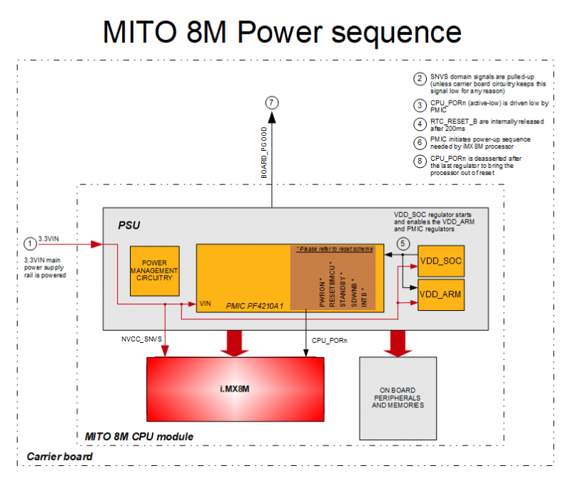
MITO 8M SOM simplifies this task by embedding all the needed circuitry. The following picture shows a simplified block diagram of PSU/voltage monitoring circuitry:
The PSU is composed of two main blocks:
- power management integrated circuit
- additional generic power management circuitry that completes PMIC functionalities
The PSU:
- generates the proper power-up sequence required by the SOC processor and surrounding memories and peripherals
- synchronizes the powering up of carrier board in order to prevent back power
Power-up sequence[edit | edit source]
The typical power-up sequence is the following:
- 3.3VIN main power supply rail is powered
- SNVS domain signals are pulled-up (unless carrier board circuitry keeps this signal low for any reason)
- CPU_PORn (active-low) is driven low by PMIC
- RTC_RESET_B are internally released after 200ms
- VDD_SOC regulator starts and enables the VDD_ARM and PMIC regulators
- PMIC initiates power-up sequence needed by iMX8M processor
- BOARD_PGOOD goes up when NVCC_3V3 (CPU I/O power rail) is ready
- CPU_PORn is deasserted after the last regulator to bring the processor out of reset
Note on BOARD_PGOOD usage[edit | edit source]
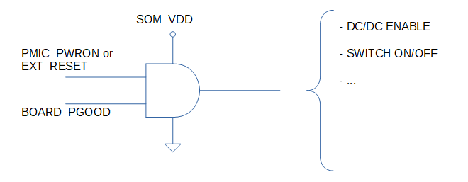
BOARD_PGOOD is generally used on carrier board to drive loads such as DC/DC enable inputs or switch on/off control signals.
Depending on the kind of such loads, BOARD_PGOOD might not be able to drive them properly because it has a 20mA output current absolute maximum rating.
In these cases a simple 2-input AND port can be used to address this issue. The following picture depicts a principle schematic showing this solution.
Additionally, we suggest using an IC with Schmitt trigger input ports.
Reset scheme and control signals[edit | edit source]
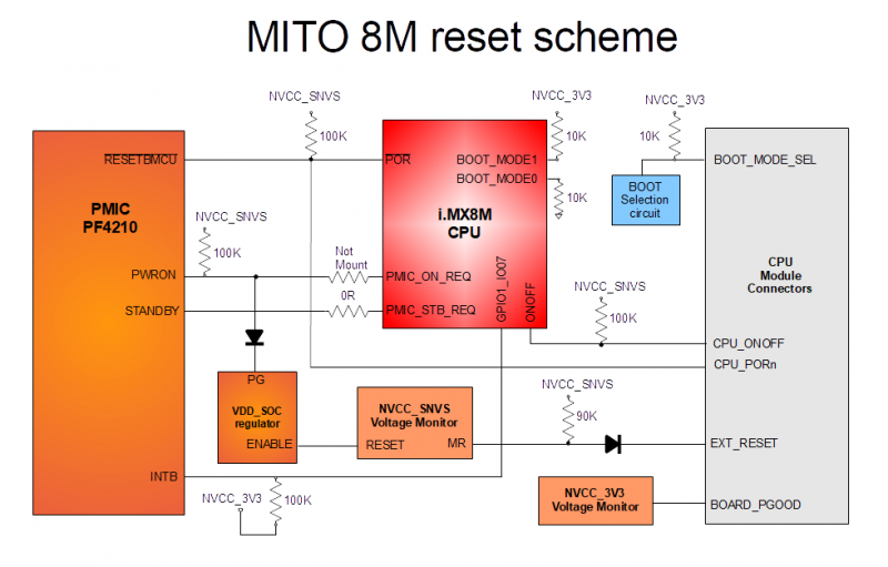
The following picture shows the simplified block diagram of reset scheme and voltage monitoring.
NVCC_VSNVS[edit | edit source]
Some signals that are related to reset circuitry are pulled-up to NVCC_VSNVS (aka 3.3VIN).
Hence it is recommended that system designer takes into account these factors in order to properly manage these signals at carrier board level.
EXT_RESET[edit | edit source]
EXT_RESET is internally pulled-up with a 90kΩ to NVCC_VSNVS. Connect EXT_RESET signal to GND (for example with a button or an open-collector circuit) causes the internal supervisor IC to assert its RESETn output.
This will power down the VDD_SOC_0V9 and make PMIC_ON pulled low by PG (Power Good) of VDD_SOC_0V9 regulator.
Since PMIC_ON serves as the enable signal of PMIC and other discrete power supply chips, all the power supplies except for the SNVS domain will be OFF.
The RESETn will keep asserted for 270 ms after EXT_RESET is released, thus providing enough time for the power supplies to be completely powered down. During this time, the POR_B driven by the PMIC will also keep asserted (low).
After RESETn is released, the power supplies will start to ramp up in defined sequence. When all the power supplies have reached their operating voltages, POR_B will be de-asserted, and the CPU may begin booting from reset.
CPU_PORn[edit | edit source]
PMIC can assert this active-low signal. Other internal IC, such as ethernet PHY or boot memory devices, could be connected to this signal. This guarantees it is in a known state when reset signal is released.
CPU_ONOFF[edit | edit source]
CPU_ONOFF is internally pulled-up with a 100kΩ to NVCC_VSNVS. This input signal is connected directly to the ONOFF input of the CPU.
BOARD_PGOOD[edit | edit source]
BOARD_PGOOD is directly related to the internal NVCC_3V3 rail (I/O pins supply) presence and must be used as power enable for all the electronics on MITO 8M carrier board.
When the I/O pins power rail on MITO 8M is not ready (BOARD_PGOOD low) all the integrated circuits connected to the CPU must be powered off in order to avoid back-powering or other issue related to a wrong power-up sequence.
BOOT_MODE_SEL[edit | edit source]
BOOT_MODE_SEL is internally pulled-up with a 100kΩ to NVCC_3V3.
When connected to GND, select the external microSD as the boot device.
Handling CPU-initiated software reset[edit | edit source]
By default, MX8 processor does not assert any external signal when it initiates a software reset sequence. Also default software reset implementation does not guarantee that all processor registers are reset properly.
For these reasons it is strongly recommended to use a different approach that, in combination with the use of a processor's watchdog timer (WDT), provides a full hardware reset in case a software reset is issued.
This technique is implemented in DESK-MX8M-L. At the software level, U-Boot and Linux kernel software reset routines make use of the processor's WDT to assert the WDOG_B signal. This signal in turn is routed to the GPIO1_IO02 pad. At the hardware level, this signal is AC-coupled to the master reset pin of the internal supervisor IC. It acts as a complete hardware reset by the assertion of its RESETn output (on the same way of EXT_RESET pin).
System boot[edit | edit source]
The boot process begins at Power On Reset (POR) where the hardware reset logic forces the ARM core to begin execution starting from the on-chip boot ROM. The boot ROM:
- determines whether the boot is secure or non-secure
- performs some initialization of the system and clean-ups
- reads the mode pins to determine the primary boot device
- once it is satisfied, it executes the boot code
Boot options[edit | edit source]
Two options are available related to system boot. They are identified by the Boot field of the ordering code as follows:
- 0: eMMC / SD option (SOM code: DMIxxx0xxxxR)
- 1: NAND / SD option (SOM code: DMIxxx1xxxxR)
For both options the selection of primary boot device is determined by the BOOT_MODE_SEL signal as described in the following sections. BOOT_MODE_SEL is latched when processor reset is released.
In any case, boot process is managed by on-chip boot ROM code that is described in detail in processor's Reference Manual.
eMMC / SD option[edit | edit source]
Selection of primary boot device is determined by the BOOT_MODE_SEL signal as follows:
- BOOT_MODE_SEL = 0
- primary boot device is SD2 (USDHC2)
- boot ROM will try to boot a valid image from the SD card. In case no valid image is found, boot ROM shall enable USB serial download mode automatically
- BOOT_MODE_SEL = 1 or floating
- primary boot device is eMMC connected to USDHC1
- in case no valid image is found on eMMC, boot ROM shall enable USB serial download mode automatically
NAND / SD option[edit | edit source]
Selection of primary boot device is determined by the BOOT_MODE_SEL signal as follows:
- BOOT_MODE_SEL = 0
- primary boot device is SD2 (USDHC2)
- in case no valid image is found in SD card, boot ROM shall enable USB serial download mode automatically
- BOOT_MODE_SEL = 1 or floating
- primary boot device is NAND flash
- in case no valid image is found in NAND flash, boot ROM shall enable USB serial download mode automatically
Important note for manufacture mode management[edit | edit source]
When the internal boot and recover boot (if enabled) failed, the boot goes to the SD/MMC manufacture mode before the serial download mode.
By default, the SD/MMC manufacture mode is enabled. DAVE Embedded Systems do not blow the fuse of the DISABLE_SDMMC_MFG in order to disable it.
Boot ROM detect SD/MMC card on USDHC2 port. If a card is inserted, ROM will try to boot from it. SD2_CD_B is used as card detect signal during bootrom's manufacture mode. This signal need to be kept high during bootstrap stage in order to prevent the intervention of bootrom's manufacture mode, if it's not desidered.
Bootstrap stage has to be intended as the time elapsing between the release of hardware reset (CPU_PORn) and the execution of the first instruction of user code (typically this is the reset vector of U-Boot boot loader).
On board JTAG connector[edit | edit source]
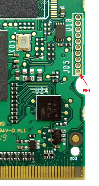
JTAG signals are routed to a dedicated connector on the MITO 8M PCB.
The connector is placed on the top side of the PCB, on the right side (please see the picture below).
JD5 - Connector's pinout[edit | edit source]
On the JF5 footprint can be hand soldered a header pinstrip 10x1x1.27mm connector. The following table reports the connector's pinout:
| Pin# | Pin name | Function | Notes |
|---|---|---|---|
| 1 | DGND | - | |
| 2 | EEPROM_WP | - | |
| 3 | NC | - | |
| 4 | JTAG_TCK | - | internal pull-up 10k to NVCC_3V3 |
| 5 | JTAG_TMS | - | |
| 6 | JTAG_TDO | - | |
| 7 | JTAG_TDI | - | |
| 8 | JTAG_nTRST | - | |
| 9 | CPU_PORn | - | internal pull-up 100k to NVCC_SNVS |
| 10 | NVCC_3V3 | - | reference voltage for JTAG signals |
Peripherals[edit | edit source]
Peripheral Audio[edit | edit source]
The Audio interface available on MITO 8M is based on iMX8M SoC which provides the following audio subsystems:
- Synchronous Audio Interface (SAI)
- 6x I2S/SAI (20+ channels, each 32-bits @384 kHz)
- Highest levels of pro audio fidelity with more than 20 audio channels each @384KHz
- Sony/Philips Digital Interface (SPDIF)
- S/PDIF Tx/Rx
Description[edit | edit source]
The I2S (or I2S) module provides a synchronous audio interface (SAI) that supports full- duplex serial interfaces with frame synchronization such as I2S, AC97, TDM, and codec/DSP interfaces. It supports the following standards and features:
- Transmitter and receiver with independent bit clock and frame sync supporting 8 data lines
- Each data line can support a maximum Frame size of 32 words
- Asynchronous 128 x 32-bit FIFO for each transmit and receive data line
- Supports packing of 8-bit and 16-bit data into each 32-bit FIFO word
- Supports combining multiple data line FIFOs into single data line FIFO
The Sony/Philips Digital Interface (SPDIF) audio block is a stereo transceiver that allows the processor to receive and transmit digital audio.
Pin mapping[edit | edit source]
The Pin mapping is described in the Pinout table section
Peripheral Ethernet[edit | edit source]
Description[edit | edit source]
The 10/100/1000-Mbit/s Ethernet interface available on MITO 8M is based on iMX8M SoC.
The SOC is directly interfaced with an ETH PHY chip (MICROCHIP KSZ9031RNX) that has the following features:
- Auto-Negotiation to Automatically Select the Highest Link-Up Speed (10/100/1000 Mbps) and Duplex (Half/Full)
- On-Chip Termination Resistors for the Differential Pairs
- Energy Detect Power-Down Mode for Reduced Power Consumption When the Cable is Not Attached
Important note for the external magnetic connection[edit | edit source]
The Ethernet peripheral requires an external insulator magnetic on the carrier board.
The four transformer center tap pins on the PHY side should not be connected to any power supply source on the board; rather, the center tap pins should be separated from one another and connected through separate 0.1 µF common-mode capacitors to ground. Separation is required because the common-mode voltage could be different between the four differential pairs, depending on the connected speed mode.
See KSZ9031RNX datasheet for more details.
Pin mapping[edit | edit source]
The Pin mapping is described in the Pinout table section
Peripheral HDMI[edit | edit source]
HDMI (High-Definition Multimedia Interface) is a compact audio/video interface for transmitting uncompressed digital video data and uncompressed/compressed digital audio data.
HDMI connects digital audio/video sources-such as set-top boxes, Blu-ray Disc players, personal computers (PCs), video game consoles, and AV receivers to compatible digital audio devices, computer monitors, and digital televisions.
Description[edit | edit source]
The HDMI interface available on MITO 8M is based on iMX8M SoC.
The HDMI port supports the following standards and features:
- High-Definition Multimedia Interface Specification, Version up to 2.0a
- Compliant with HDCP2.2 (and back compatible with HDCP1.3/HDCP1.4)
- Variety of video resolutions and formats
- Supports up to 4k2k at 60Hz resolution
- Supports 8, 10, 12, and 16bpp
- Supports RGB, YCbCr422 formats
- Variety of audio formats – PCM and compressed, over I2S interface
- I2S PCM samples are converted to comply with IEC60958 sub-frames
- Supporting I2S-TDM
Pin mapping[edit | edit source]
The Pin mapping is described in the Pinout table section
Peripheral LVDS[edit | edit source]
The LVDS interface available on MITO 8M is based on a MIPI® DSI To FLATLINK™ LVDS bridge IC.
It is directly connected to the MIPI® DSI output port of iMX8M SOC.
This support covers all aspects of these activities:
- Connectivity to relevant devices - Displays with LVDS receivers
- Arranging the data as required by the external display receiver and by LVDS display standards
- Synchronization and control capabilities
Description[edit | edit source]
The LVDS port supports the following standards and features:
- Suitable for 60-fps WUXGA 1920 × 1200 Resolution at 18-bpp and 24-bpp Color, 60 fps 1366 × 768 at 18 bpp and 24 bpp
- Output Configurable for Single-Link or Dual-Link LVDS
- LVDS Output Clock Range of 25 MHz to 154 MHz in Dual-Link or Single-Link Modes
Pin mapping[edit | edit source]
The Pin mapping is described in the Pinout table section
Peripheral MIPI[edit | edit source]
The MIPI interfaces available on iMX8M SoC are following described:
- The Camera Serial Interface (CSI) is a specification of the Mobile Industry Processor Interface (MIPI) Alliance. It defines an interface between a camera and a host processor.
- The Display Serial Interface (DSI) is a specification by the Mobile Industry Processor Interface (MIPI) Alliance aimed at reducing the cost of display controllers in a mobile device. It is commonly targeted at LCD and similar display technologies.
The two CSI interface on MITO 8M SOM:
- CSI1 is avaiable on SODIMM connector pinout
- CSI2 is avaiable on ONE PIECE expansion connector J5
The DSI interface is internally used on MITO 8M SOM to generate an LVDS output interface. More details on LVDS section.
Description[edit | edit source]
The MIPI CSI port supports the following standards and features:
- Configurable interface logic to support most commonly available CMOS sensors.
- Scalable data lane support, 1 to 4 Data Lanes
- Support for CCIR656 video interface as well as traditional sensor interface.
- 8-bit / 16-bit / 24-bit data port for YCbCr, YUV, or RGB data input.
- 8-bit / 10-bit / 16-bit data port for Bayer data input.
- Implements all three CSI-2 MIPI layers (Pixel to byte packing, low level protocol, Lane management)
Pin mapping[edit | edit source]
The Pin mapping is described in the Pinout table section
Peripheral SDIOs[edit | edit source]
The Ultra Secured Digital Host Controller (uSDHC) provides the interface between the host system and the SD/SDIO/MMC cards or devices.
MITO 8M SOM provides up to two SDIO interface available for an external memory device connection.
The availability of this interface is related to the SOM mounting option:
- on NAND on board version, the NAND interface is internally connected, and the SD1 interface is routed externally the SOM
- on eMMC on board version, the SD1 interface is internally connected, and the NAND interface is routed externally the SOM
See Pin mapping tables for connection details.
Description[edit | edit source]
The SDIOs interface available on MITO 8M is based on iMX8M SoC.
The SDIOs port supports the following standards and features:
- Conforms to the SD Host Controller Standard Specification version 2.0/3.0
- Compatible with the MMC System Specification version 4.2/4.3/4.4/4.41/5.0/5.1
- Compatible with the SD Memory Card Specification version 3.0 and supports the Extended Capacity SD Memory Card
- Compatible with the SDIO Card Specification version 2.0/3.0
- Supports 1-bit/4-bit SD and SDIO modes, and 1-bit/4-bit/8-bit MMC modes
- Card bus clock frequency up to 208 MHz
Pin mapping[edit | edit source]
The Pin mapping is described in the Pinout table section
Peripheral UARTs[edit | edit source]
Description[edit | edit source]
The Universal Asynchronous Receiver/Transmitter (UART) interface available on MITO 8M is based on iMX8M SoC.
UARTs provides serial communication capability with external devices and support NRZ encoding format, RS485 compatible 9 bit data format and IrDA-compatible infrared slow data rate (SIR) format.
The UART port supports the following standards and features:
- High-speed TIA/EIA-232-F compatible, up to Mbit/s
- Serial IR interface low-speed, IrDA-compatible (up to 115.2 Kbit/s)
- 9-bit or Multidrop mode (RS-485) support (automatic slave address detection)
- 7 or 8 data bits for RS-232 characters, or 9 bit RS-485 format
- 1 or 2 stop bits
- Programmable parity (even, odd, and no parity)
- Hardware flow control support for request to send (RTS_B) and clear to send (CTS_B) signals
- Two independent, 32-entry FIFOs for transmit and receive
Pin mapping[edit | edit source]
The Pin mapping is described in the Pinout table section
Peripheral USB[edit | edit source]
Universal Serial Bus (USB) is an industry standard that establishes specifications for cables and connectors and protocols for connection, communication and power supply (interfacing) between computers, peripherals and other computers.
Description[edit | edit source]
The two USB interface available on MITO 8M are based on iMX8M SoC.
Each USB 3.0-compliant serial interface port supports the following standards and features:
- USB dual-role operation and can be configured as host or device
- Super-speed (5 Gbit/s), high-speed (480 Mbit/s), full-speed (12 Mbit/s), and low-speed (1.5 Mbit/s) operations.
- OTG (on-the-go) 2.0 compliant, which includes both device and host capability. Super-speed operation is not supported when OTG is enabled.
Pin mapping[edit | edit source]
The Pin mapping is described in the Pinout table section
Peripheral PCI Express[edit | edit source]
PCI Express (Peripheral Component Interconnect Express) is a high-speed serial computer expansion bus standard, designed to replace the older PCI, PCI-X and AGP bus standards.
The two PCI Express interface on MITO 8M SOM:
- PCIe1 is avaiable on SODIMM connector pinout
- PCIe2 is avaiable on ONE PIECE expansion connector J5
Description[edit | edit source]
The PCI Express interfaces available on MITO 8M is based on iMX8M SoC.
The PCI Express interfaces supports the following standards and features:
- two PCIe PHY ports (1-lines each)
- up to 6.0 Gbps data rate
- complies to PCI Express base specification 2.1.
- 8B/10B Encoding / Decoding
- Supports Spread Spectrum Clocking in Transmitter and Receiver
Pin mapping[edit | edit source]
The Pin mapping is described in the Pinout table section
Peripheral GPIOs[edit | edit source]
The GPIO general-purpose input/output peripheral provides dedicated general-purpose pins that can be configured as either inputs or outputs.
Description[edit | edit source]
When configured as an output, it is possible to write to an internal register to control the state driven on the output pin. When configured as an input, it is possible to detect the state of the input by reading the state of an internal register. In addition, the GPIO peripheral can produce CORE interrupts.
Pin mapping[edit | edit source]
The Pin mapping is described in the Pinout table section
Real Time Clock[edit | edit source]
This chapter describes the technical specifications and features for the RTC component on the MITO 8M module.
The Real Time Clock available on MITO 8M is based on iMX8M SoC.
Features[edit | edit source]
The MITO 8M module uses a 32.768kHz dedicated crystal in order to obtain an accurate time base for the RTC.
Important note for RTC during power-off[edit | edit source]
On the MITO 8M module the SNVS voltage rails are obtained by the main supply of the SOM.
For this reason, there is no possibility to keep operative the CPU RTC when the SOM is not connected to the 3.3VIN power rail.
Use an external RTC with battery backup functionality if required.
Peripheral Watchdog[edit | edit source]
The Watchdog Timer (WDOG) protects against system failures by providing a method by which to escape from unexpected events or programming errors.
Description[edit | edit source]
By default, the Watchdog Timer of iMX8M SOC is internally used on MITO 8M for the CPU-initiated software reset function.
For more details see the reset scheme and control signals section.
Pin mapping[edit | edit source]
The Pin mapping is described in the Pinout table section
Electrical, Thermal and Mechanical Features[edit | edit source]
Operational characteristics[edit | edit source]
Maximum ratings[edit | edit source]
| Parameter | Min | Typ | Max | Unit |
|---|---|---|---|---|
| Main power supply voltage | 0 | 3.3 | 3.6 | V |
Recommended ratings[edit | edit source]
| Parameter | Min | Typ | Max | Unit |
|---|---|---|---|---|
| Main power supply voltage | 3.135 | 3.3 | 3.465 | V |
Power consumption[edit | edit source]
Providing theoretical maximum power consumption value would be useless for the majority of system designers building their application upon MITO 8M module. Practically speaking, these figures would be of no help when it comes to size power supply unit or to perform thermal design of real systems.
Instead, several configurations have been tested in order to provide figures that are measured on real-world use cases.
Please note that MITO 8M platform is so flexible that it is virtually impossible to test for all possible configurations and applications on the market. The use cases here presented should cover most of real-world scenarios. However actual customer's application might require more power than values reported here or customer's use case may be differ significantly with respect to the ones here considered.
Therefore, application-specific requirements have always to be taken into consideration in order to size power supply unit and to implement thermal management properly.
Use cases results[edit | edit source]
Measurements have been performed on the MITO 8M SOM under test is equipped with:
| Section not completed yet |
| Checkpoint | Power (mW) |
|---|---|
| U-boot prompt | xxxx |
| Linux prompt | xxxx |
| Stress App test (*) | xxxx |
(*) Stressful Application Test: https://github.com/stressapptest/stressapptest
Thermal management[edit | edit source]
The MITO 8M SOM is designed to support the maximum available temperature range declared by the manufacturer.
The customer shall define and conduct a reasonable number of tests and verification in order to qualify the DUT capabilities to manage the heat dissipation.
Any heatsink, fan etc shall be defined case by case.
DAVE Embedded Systems' team is available for any additional information, please contact sales@dave.eu.
Heatsink suggestion[edit | edit source]
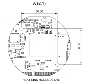
The MITO 8M SOM is designed with two holes that allow to mount a heatsink directly on the CPU IC.
Suggested part are ATS Push Pin Heat Sinks CPX0250250xx or FPX0250250xx part numbers.
See ATS website for more details [1].
Software thermal protection[edit | edit source]
In DESK-MX8-L, two software thermal protection mechanisms are implemented. Both are based on the processor's temperature sensor. It is worth remembering that maximum junction temperature (also denoted as Tj in the rest of the document) is:
- 95°C for Consumer parts
- 105°C for Industrial parts
| Section not completed yet |
U-Boot[edit | edit source]
At U-Boot level, automatic boot procedure is halted until Tj is smaller than (following temperatures might seem excessively low but they take into account the intrinsic poor precision of the temperature sensor to provide a reasonable safe margin):
- TBD for Consumer parts
- 95°C for Industrial parts
Linux kernel[edit | edit source]
At Linux level, a more sophisticated protection mechanism is implemented. Please refer to the following sections for more details.
The default temperature thresholds depend on the silicon grade, as follows:
- for Consumer parts
- passive threshold: TBD
- critical threshold: TBD
- for Industrial parts
- passive threshold: 85°C
- critical threshold: 95°C
Practically speaking, for DESK-MX8-L this mechanism makes use of two different thresholds, denoted as trip_point0 (also known as passive threshold) and trip_point1 (also known as critical threshold).
When Tj reaches trip_point0, Linux kernel scales down processor frequency.
If Tj reaches trip_point1, a complete shutdown is triggered:
thermal thermal_zone0: critical temperature reached(95 C),shutting down
By default, temperature thresholds are set up as follows:
trip_point0: 85°Ctrip_point1: 95°C.
Trip point thresholds can be accessed via sysfs interface from user space. The following example shows how to read the values of the trip points:
root@mito:~# cat /sys/devices/virtual/thermal/thermal_zone0/trip_point_0_temp
85000
root@mito:~# cat /sys/devices/virtual/thermal/thermal_zone0/trip_point_1_temp
950000
This example shows how to set trip points 0 and 1 to 95°C and 100°C respectively:
echo 95000 > /sys/class/thermal/thermal_zone0/trip_point_0_temp
echo 100000 > /sys/class/thermal/thermal_zone0/trip_point_1_temp
Please note that:
- it is possible to set up trip points greater than the maximum junction temperature indicated by manufacturer datasheet;
- exceeding maximum junction temperature indicated by manufacturer datasheet may cause permanent damage.
To read current processor temperature please issue this command (reported temperature is 36.676°C in the example):
root@mito:~# cat /sys/class/thermal/thermal_zone0/temp
36676
For more details about this functionality, please refer to Documentation/thermal/sysfs-api.txt in the kernel sources.
Mechanical specifications[edit | edit source]
This chapter describes the mechanical characteristics of the MITO 8M module.
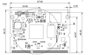
Board Layout[edit | edit source]
The following figure shows the physical dimensions of the MITO 8M module:
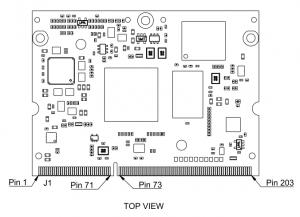
Connectors[edit | edit source]
The following figure shows the MITO 8M connector layout:
CAD drawings[edit | edit source]
- DXF (2D): CS031518.dxf
- STEP (3D): CS031518
