DWM ADD-ON/DWM Hardware/pdf
General Information[edit | edit source]
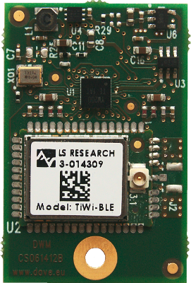
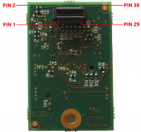
DWM TOP View[edit | edit source]
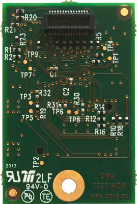
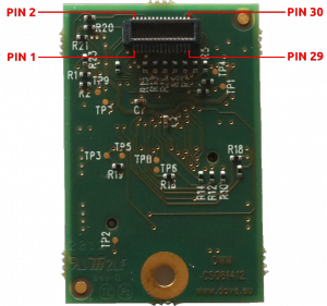
DWM BOTTOM View[edit | edit source]
Introduction[edit | edit source]
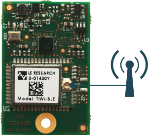
The module is built around an LS Research TiWi-BLE Integrated Transceiver Modules for WLAN 802.11 b/g/n and Bluetooth. The module implements the necessary PHY/MAC layers to support WLAN applications in conjunction with a host processor over a SDIO interface. The module also provides a Bluetooth platform through the HCI transport layer. Both WLAN and Bluetooth share the same antenna port.
Features[edit | edit source]
- Based on Texas Instruments WL1271L Transceiver
- IEEE 802.11 b,g,n,d,e,i, compliant
- Bluetooth 2.1+EDR, Power Class 1.5
- Full support for BT4.0 BLE and ANT
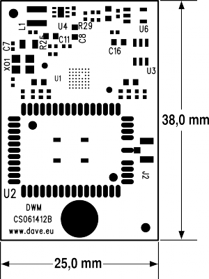
- Reduced footprint: 25 mm x 38 mm
- Low height profile
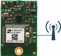
- U.FL connector for external antenna
- Integrated band-pass filter
- Industrial operating temperature range: -40 / +85 °C
Interface timings[edit | edit source]
Please refer to the TiWi-BLE Datasheet for SDIO [WiFi] and UART [Bluetooth] interface timings.
Hardware versioning and tracking[edit | edit source]
DWM ADD-ON implements well established versioning and tracking mechanisms:
- PCB version is copper printed on PCB itself, as shown in Fig. 1
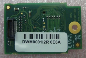
- serial number: it is printed on a white label, as shown in Fig. 2: see also Product serial number page for more details
Part number composition[edit | edit source]
DWM ADD-ON part number is identified by the following digit-code table:
| Part number structure | Options | Description |
|---|---|---|
| DWM | Prefix | |
| RFU |
|
Reserved for future use |
| Temperature range |
|
For the DAVE Embedded Systems' product Temperature Range classification, please find more information at the page Products Classification |
| PCB revision |
|
PCB release may change for manufacturing purposes (i.e. text fixture adaptation) |
| Manufacturing option |
|
typically connected to production process and quality |
Example[edit | edit source]
DWM ADD-ON code DWM0001I2R
- DWM - DWM ADD-ON
- 0001 - standard version
- I - Industrial grade
Pinout Table[edit | edit source]
Connectors and Pinout Table[edit | edit source]
Connectors description[edit | edit source]
In the following table are described all available connectors integrated on DWM_ADD-ON:
| Connector name | Connector Type | Notes | Carrier board counterpart |
|---|---|---|---|
| J1 | Dual in line low profile high density connector 30pins | Molex 501920-3001 | Molex 52991-030, others are available with different stand-off |
| Antenna's connector | UFL type | N.A. | UFL cable side (many versions available in the marked already inserted on cables/antenna patches) |
The dedicated carrier board must mount the mating connector and connect the desired peripheral interfaces according to DWM pinout specifications. See the images below for reference:
Pinout table naming conventions[edit | edit source]
This chapter contains the pinout description of the DWM module, grouped in two tables (odd and even pins) that report the pin mapping of the TBD: connector type DWM connector.
Each row in the pinout tables contains the following information:
| Pin | Reference to the connector pin |
| Pin Name | Pin (signal) name on the DWM connectors |
| Internal connections |
Connections to the DWM components
|
| Ball/pin # | Component ball/pin number connected to signal |
| Voltage | I/O voltage levels |
| Type | Pin type:
|
| Notes | Remarks on special pin characteristics |
| Pin MUX alternative functions | Muxes:
The number of functions depends on platform |
Pinout Table ODD pins declaration[edit | edit source]
| Pin | Pin Name | Internal Connections | Ball/pin # | Voltage domain | Type | Notes | Pin MUX alternative functions |
| J1.1 | BT_EN | Bluetooth Enable | 3.3V | I | |||
| J1.3 | BT_CTS | Bluetooth HCI UART CTS | 3.3V | I | |||
| J1.5 | BT_RX | Bluetooth HCI UART RX | 3.3V | I | |||
| J1.7 | BT_RTS | Bluetooth HCI UART RTS | 3.3V | O | |||
| J1.9 | BT_TX | Bluetooth HCI UART TX | 3.3V | O | |||
| J1.11 | DGND | Ground | - | G | |||
| J1.13 | DAT3 | SDIO Data Bit 3 | 3.3V | D | |||
| J1.15 | DAT2 | SDIO Data Bit 2 | 3.3V | D | |||
| J1.17 | DAT1 | SDIO Data Bit 1 | 3.3V | D | |||
| J1.19 | DAT0 | SDIO Data Bit 0 | 3.3V | D | |||
| J1.21 | DGND | Ground | - | G | |||
| J1.23 | SDO_CMD | SDIO Command Line | 3.3V | I/O | |||
| J1.25 | DGND | Ground | - | G | |||
| J1.27 | 3.3V | +3.3V Input Voltage | 3.3V | S | |||
| J1.29 | 5V | +5V Input Voltage | 5V | S |
Pinout Table EVEN pins declaration[edit | edit source]
| Pin | Pin Name | Internal Connections | Ball/pin # | Voltage domain | Type | Note | Pin MUX alternative functions |
| J1.2 | WIFI_EN | WLAN Enable | 3.3V | I | |||
| J1.4 | WIFI_IRQ | WLAN Interrupt Request | 3.3V | O | |||
| J1.6 | BT_F2 | Bluetooth Wakeup | 3.3V | I | Please leave unconnected if not used | ||
| J1.8 | WIFI_CLK_REQ(A) | HOST_WakeUp | 3.3V | O | Please leave unconnected if not used | ||
| J1.10 | NC | Reserved for future use | - | Please leave unconnected. | |||
| J1.12 | NC | Reserved for future use | - | Please leave unconnected. | |||
| J1.14 | NC | Reserved for future use | - | Please leave unconnected. | |||
| J1.16 | NC | Reserved for future use | - | Please leave unconnected. | |||
| J1.18 | NC | Reserved for future use | - | Please leave unconnected. | |||
| J1.20 | NC | Reserved for future use | - | Please leave unconnected. | |||
| J1.22 | DGND | Ground | - | G | |||
| J1.24 | SDO_CLK | SDIO Clock | 3.3V | I | |||
| J1.26 | DGND | Ground | - | G | |||
| J1.28 | 3.3V | +3.3V Input Voltage | 3.3V | S | |||
| J1.30 | 5V | +5V Input Voltage | 5V | S |
Electrical, Thermal and Mechanical Features[edit | edit source]
Operational characteristics[edit | edit source]
Maximum ratings[edit | edit source]
| Parameter | Min | Typ | Max | Unit |
|---|---|---|---|---|
| Main power supply voltage | -0.3 | 3.3 | 3.6 | V |
Recommended ratings[edit | edit source]
| Parameter | Min | Typ | Max | Unit |
|---|---|---|---|---|
| Main power supply voltage | 3.135 | 3.3 | 3.465 | V |
Mechanical specifications[edit | edit source]
This chapter describes the mechanical characteristics of the DWM module.
Board Layout[edit | edit source]
The following figure shows the physical dimensions of the DWM module:
Connectors[edit | edit source]
The following figure shows the DWM connector layout:
