

|
The information here provided are preliminary and subject to change.
|
|
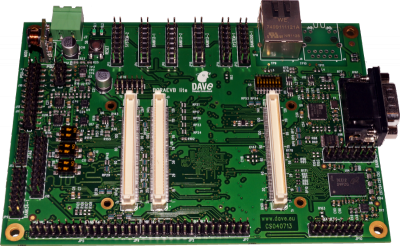
BoraEVB-Lite is a carrier board designed to host Bora system-on-module.
The following picture shows Bora-EVB-Lite's block diagram:
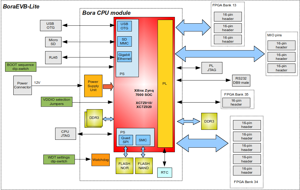
- 10/100/1000 Ethernet
- 1x USB OTG
- Serial port (RS232)
- 1x MicroSD
- External DDR3 SDRAM bank
- +12V power connector
- JTAG
- 2.54mm-pitch pin-strip connectors for Bora PS and PL configurable peripherals (MIO and EMIO interfaces, GPIOs, custom IPs, ..)
Board version CS040713 has the following limitations:
- USB OTG is not available
- MicroSD is not available
- DDR3 bank is not available
| Pin#
|
Pin name
|
Function
|
Notes
|
| 1, 10, 11, 16 |
DGND |
Ground |
-
|
| 2 |
IO_L19P_T3_34 |
- |
-
|
| 3 |
IO_L2P_T0_34 |
- |
-
|
| 4 |
IO_L19N_T3_VREF_34 |
- |
-
|
| 5 |
IO_L2N_T0_34 |
- |
-
|
| 6 |
IO_L18P_T2_34 |
- |
-
|
| 7 |
IO_L22P_T3_34 |
- |
-
|
| 8 |
IO_L18N_T2_34 |
- |
-
|
| 9 |
IO_L22N_T3_34 |
- |
-
|
| 12 |
IO_L15P_T2_DQS_34 |
- |
-
|
| 13 |
IO_L8P_T1_34 |
- |
-
|
| 14 |
IO_L15N_T2_DQS_34 |
- |
-
|
| 15 |
IO_L8N_T1_34 |
- |
-
|
| Pin#
|
Pin name
|
Function
|
Notes
|
| 1 |
PS_MIO28_501 |
- |
-
|
| 2, 10, 7, 15 |
DGND |
Ground |
-
|
| 3 |
PS_MIO29_501 |
- |
-
|
| 4 |
PS_MIO34_501 |
- |
-
|
| 5 |
PS_MIO30_501 |
- |
-
|
| 6 |
PS_MIO35_501 |
- |
-
|
| 8 |
PS_MIO36_501 |
- |
-
|
| 9 |
PS_MIO31_501 |
- |
-
|
| 11 |
PS_MIO32_501 |
- |
-
|
| 12 |
PS_MIO37_501 |
- |
-
|
| 13 |
PS_MIO33_501 |
- |
-
|
| 14 |
PS_MIO38_501 |
- |
-
|
| 16 |
PS_MIO39_501 |
- |
-
|
| Pin#
|
Pin name
|
Function
|
Notes
|
| 1, 10, 11, 16 |
DGND |
Ground |
-
|
| 2 |
IO_L9P_T1_DQS_34 |
- |
-
|
| 3 |
IO_L21P_T3_DQS_34 |
- |
-
|
| 4 |
IO_L9N_T1_DQS_34 |
- |
-
|
| 5 |
IO_L21N_T3_DQS_34 |
- |
-
|
| 6 |
IO_L7P_T1_34 |
- |
-
|
| 7 |
IO_L20P_T3_34 |
- |
-
|
| 8 |
IO_L7N_T1_34 |
- |
-
|
| 9 |
IO_L20N_T3_34 |
- |
-
|
| 12 |
N.A. |
N.A. |
-
|
| 13 |
IO_L1P_T0_34 |
- |
-
|
| 14 |
IO_L6N_T0_VREF_34 |
- |
-
|
| 15 |
IO_L1N_T0_34 |
- |
-
|
| Pin#
|
Pin name
|
Function
|
Notes
|
| 1, 10, 11, 16 |
DGND |
Ground |
-
|
| 2 |
IO_L5P_T0_34 |
- |
-
|
| 3 |
IO_L17P_T2_34 |
- |
-
|
| 4 |
IO_L5N_T0_34 |
- |
-
|
| 5 |
IO_L17N_T2_34 |
- |
-
|
| 6 |
IO_L4P_T0_34 |
- |
-
|
| 7 |
IO_L16P_T2_34 |
- |
-
|
| 8 |
IO_L4N_T0_34 |
- |
-
|
| 9 |
IO_L16N_T2_34 |
- |
-
|
| 12 |
IO_L24P_T3_34 |
- |
-
|
| 13 |
IO_L23P_T3_34 |
- |
-
|
| 14 |
IO_L24N_T3_34 |
- |
-
|
| 15 |
IO_L23N_T3_34 |
- |
-
|
| Pin#
|
Pin name
|
Function
|
Notes
|
| 1, 10, 11, 16 |
DGND |
Ground |
-
|
| 2 |
IO_L16P_T2_13 |
- |
-
|
| 3 |
IO_L20P_T3_13 |
- |
-
|
| 4 |
IO_L16N_T2_13 |
- |
-
|
| 5 |
IO_L20N_T3_13 |
- |
-
|
| 6 |
IO_L22P_T3_13 |
- |
-
|
| 7 |
IO_L17P_T2_13 |
- |
-
|
| 8 |
IO_L22N_T3_13 |
- |
-
|
| 9 |
IO_L17N_T2_13 |
- |
-
|
| 12, 14 |
VDDIO_BANK13 |
- |
-
|
| 13 |
IO_L19P_T3_13 |
- |
-
|
| 15 |
IO_L19N_T3_VREF_13 |
- |
-
|
| Pin#
|
Pin name
|
Function
|
Notes
|
| 1, 6, 11, 12 |
DGND |
Ground |
-
|
| 2 |
IO_L14P_T2_SRCC_34 |
- |
-
|
| 3 |
N.A. |
N.A. |
-
|
| 4 |
IO_L14N_T2_SRCC_34 |
- |
-
|
| 5 |
N.A. |
N.A. |
-
|
| 7 |
N.A. |
N.A. |
-
|
| 8 |
IO_L11P_T1_SRCC_34 |
- |
-
|
| 9 |
N.A. |
N.A. |
-
|
| 10 |
IO_L11N_T1_SRCC_34 |
- |
-
|
| 13 |
IO_L3P_T0_DQS_PUDC_B_34 |
- |
-
|
| 14, 16 |
N.C. |
Not connected |
-
|
| 15 |
IO_L3N_T0_DQS_34 |
- |
-
|
| Pin#
|
Pin name
|
Function
|
Notes
|
| 1, 7, 10, 13, 16 |
DGND |
Ground |
-
|
| 2 |
IO_L21P_T3_DQS_13 |
- |
-
|
| 3 |
IO_L15P_T2_DQS_13 |
- |
-
|
| 4 |
IO_L21N_T3_DQS_13 |
- |
-
|
| 5 |
IO_L15N_T2_DQS_13 |
- |
-
|
| 6 |
IO_L18P_T2_13 |
- |
-
|
| 8 |
IO_L18N_T2_13 |
- |
-
|
| 9 |
IO_L11P_T1_SRCC_13 |
- |
-
|
| 11 |
IO_L11N_T1_SRCC_13 |
- |
-
|
| 12 |
IO_L13P_T2_MRCC_13 |
- |
-
|
| 14 |
IO_L13N_T2_MRCC_13 |
- |
-
|
| 15 |
VDDIO_BANK13 |
- |
-
|
| Pin#
|
Pin name
|
Function
|
Notes
|
| 1, 7, 13 |
DGND |
Ground |
-
|
2, 4, 6, 8, 10
12, 14, 15, 16 |
N.C. |
Not connected |
-
|
| 3 |
IO_L12P_T1_MRCC_34 |
- |
-
|
| 5 |
IO_L12N_T1_MRCC_34 |
- |
-
|
| 9 |
IO_L13P_T2_MRCC_34 |
- |
-
|
| 11 |
IO_L13N_T2_MRCC_34 |
- |
-
|
| Pin#
|
Pin name
|
Function
|
Notes
|
| 1 |
IO_0_35 |
- |
-
|
| 2, 4 |
VDDIO_BANK35 |
- |
-
|
| 3, 6, 9, 12, 15 |
XADC_GND |
- |
-
|
| 5 |
ZYNQ_AD14P_35 |
- |
-
|
| 7 |
ZYNQ_AD14N_35 |
- |
-
|
| 8 |
ZYNQ_T0_VREF_35 |
- |
-
|
| 10 |
ZYNQ_T3_VREF_35 |
- |
-
|
| 11 |
ZYNQ_AD1P_35 |
- |
-
|
| 13 |
ZYNQ_AD1N_35 |
- |
-
|
| 14 |
ZYNQ_AD3P_35 |
- |
-
|
| 16 |
ZYNQ_AD3N_35 |
- |
-
|
| Pin#
|
Pin name
|
Function
|
Notes
|
| 1, 10, 11, 16 |
DGND |
Ground |
-
|
| 2 |
xxx |
- |
-
|
| 3 |
xxx |
- |
-
|
| 4 |
xxx |
- |
-
|
| 5 |
xxx |
- |
-
|
| 6 |
xxx |
- |
-
|
| 7 |
xxx |
- |
-
|
| 8 |
xxx |
- |
-
|
| 9 |
xxx |
- |
-
|
| 10 |
xxx |
- |
-
|
| 11 |
xxx |
- |
-
|
| 12 |
xxx |
- |
-
|
| 13 |
xxx |
- |
-
|
| 14 |
xxx |
- |
-
|
| 15 |
xxx |
- |
-
|
| 16 |
xxx |
- |
-
|
| Pin#
|
Pin name
|
Function
|
Notes
|
| 1 |
VDDIO_BANK13 |
- |
-
|
| 2, 4, 7, 13, 14 |
xxx |
- |
-
|
| 3 |
IO_L14P_T2_SRCC_13 |
- |
-
|
| 5 |
IO_L14N_T2_SRCC_13 |
- |
-
|
| 6 |
ZYNQ_L6N_T0_VREF_13 |
- |
-
|
| 8, 10, 12, 15, 16 |
DGND |
Ground |
-
|
| 9 |
IO_L12P_T1_MRCC_13 |
- |
-
|
| 11 |
IO_L12N_T1_MRCC_13 |
- |
-
|
- ORCAD: coming soon
- PDF: coming soon
- DXF: coming soon
- IDF (3D): coming soon


